Nitride semiconductor wafer and method of processing nitride semiconductor wafer

a technology of nitride semiconductor and semiconductor wafer, which is applied in the direction of semiconductor/solid-state device details, manufacturing tools, lapping machines, etc., can solve the problems of sapphire wafers with high mechanical rigidity, and sapphire wafers with weak points

Inactive Publication Date: 2005-07-07
SUMITOMO ELECTRIC IND LTD +1
View PDF8 Cites 13 Cited by
  • Summary
  • Abstract
  • Description
  • Claims
  • Application Information

AI Technical Summary

Benefits of technology

[0067] The conventional GaN wafers had a roughened bottom surface which is likely to attract particles and allow them to adhere thereon. The present invention polishes also a bottom surface into mirror smoothness. A smoothed bottom surface of a nitride wafer of the present invention is immune from particle contamination. Reduction of the particle contamination is an advantage of the present invention. Another advantage derives from small TTV (total thickness variation) less than 10 μm (TTV≦10 μm). The thickness of the wafer is nearly constant allover on the surface. The small TTV can suppress the fluctuation of properties of devices made upon the wafers. For example, surface morphology after epitaxial film-growth is improved by the low fluctuation of thickness (TTV) realized by the present invention.
. Another advantage derives from small TTV (total thickness variation) less than 10 μm (TTV≦10 μm). The thickness of the wafer is nearly constant allover on the surface. The small TTV can suppress the fluctuation of properties of devices made upon the wafers. For example, surface morphology after epitaxial film-growth is improved by the low fluctuation of thickness (TTV) realized by the present invention.

Problems solved by technology

Sapphire wafers, however, have weak points.
The top electrode is one drawback of sapphire wafers.
High mechanical rigidity is a further drawback for sapphire wafers.
Without relying upon natural cleavage, a device-produced sapphire wafer is cut into individual chips by mechanical dicing, which raises manufacturing costs and lowers yields.
Thus, the ELO fails to make a freestanding GaN substrate.
The ELO is insufficient to produce a thick single crystal GaN substrate wafer.
Polishing technology has not matured for nitride semiconductors, since independent, freestanding nitride crystal bulk wafers have not been produced on a practical scale yet.
Nobody can obtain knowledge of the detail of the alkali.
But, {circle over (9)} insisted that CMP (chemical-mechanical polishing) was still impossible for high quality GaN crystals.
The technology of making a bulk GaN single crystal wafer is not fully matured yet.
50 mmφ (2-inchφ) freestanding GaN single crystal wafers are not produced on a commercial scale and do not come onto the market yet.
However, such large GaN wafers made by the state-of-the-art technology are annoyed by poor flatness, large distortion and bad roughness.
Due to lack of a pertinent polishing method, surface roughness is over 10 μm.
No circular GaN wafers prepared by the current technology satisfy the requirements of flatness, thickness uniformity and smoothness at present yet.
GaN, however, is not tough and fragile.
It is not easy to polish chemically-tenacious, physically-rigid but fragile GaN crystals.
Slight physical shocks easily break GaN crystals.
GaN has other many problems.
A large GaN crystal is unobtainable.
The lattice misfit and thermal expansion difference cause large inner stress in the GaN film.
Distortion is a serious problem for the GaN wafers.
It is impossible to rid a wafer of distortion by the ordinary polishing.
Large wafer distortion increases difficulties in wafer process and enhances probability of breaking, splitting and cracking.
The wafer distortion makes it difficult to adjust a focus on the wafer in the masked exposure in photolithography and increases errors of patterning.
In general, lapping (grinding) and polishing (whetting) are ineffective for reducing or removing distortion from wafers.
Annihilation of distortion is a formidable problem for GaN wafers.
Another problem is fluctuation of thicknesses of wafers.
Another problem is roughness of wafer surfaces.
If fine particles once stick to rugged bottom surfaces of GaN wafers, it is very difficult to remove the particles from the rugged surfaces.
GaN freestanding bulk crystals are rigid but fragile.
The rigid-fragility of GaN incurs another problem deriving from distortion.

Method used


Image

  • Nitride semiconductor wafer and method of processing nitride semiconductor wafer
  • Nitride semiconductor wafer and method of processing nitride semiconductor wafer
  • Nitride semiconductor wafer and method of processing nitride semiconductor wafer

Examples


embodiment 1 (

[0097] [Embodiment 1 (2-inchφ GaN freestanding wafer))

[0098] 2-inchφ GaN freestanding wafers are made by an HVPE method which grows GaN films on a GaAs circular undersubstrate from a Ga-melt, HCl gas and NH3 gas in a furnace by reactions of Ga+HCl→GaCl and GaCl+NH3→GaN. The HVPE method makes the best use of the ELO (epitaxial lateral overgrowth) and the facet-growth which produces intentionally facet pits for gathering dislocations at bottoms of the pits and eliminates the GaAs undersubstrate and obtains a low-dislocation freestanding thick GaN film.

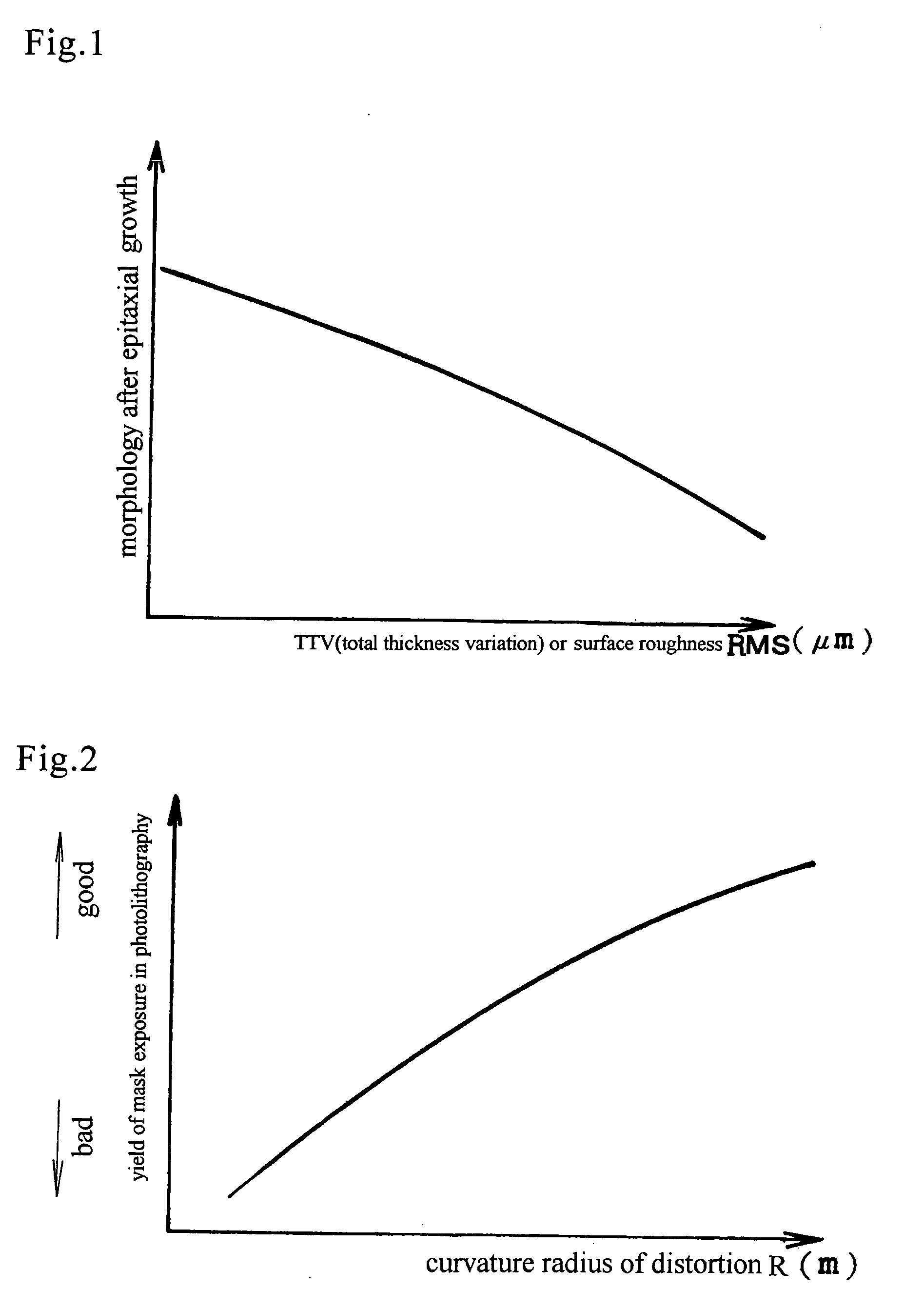
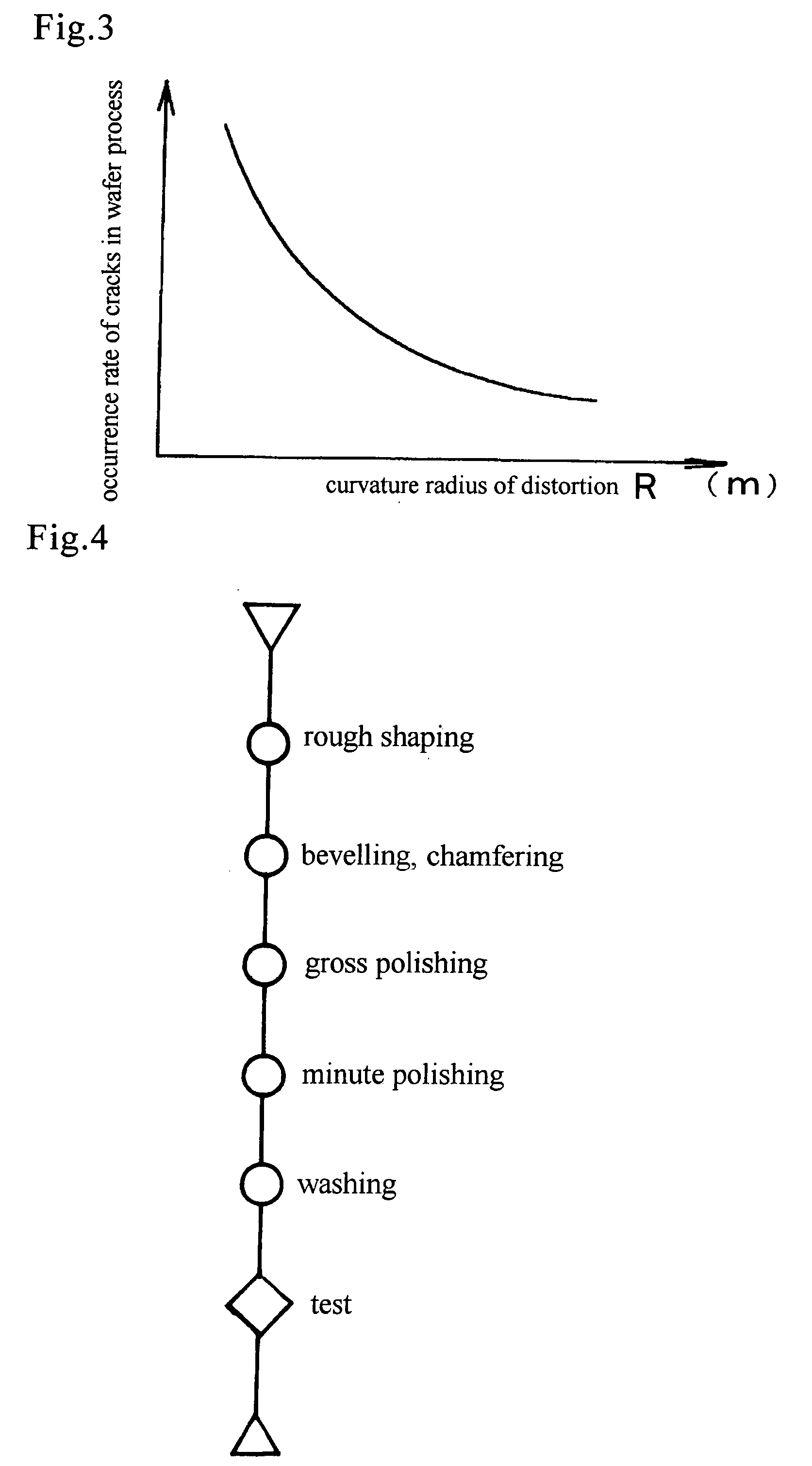
[0099] As-HVPE-grown GaN bulk wafers have rugged surfaces, random peripheral fringes, distortion and fluctuation of thickness. The rough-shaping step of FIG. 4 reforms the as-grown wafers into circular wafers by eliminating the random peripheral fringes.

[0100] The bevelling (chamfering) step of FIG. 4 eliminates sharp edges at circumferences of the circular wafers. Some of the prepared circular wafers have single-mode distortion and ot...


PUM

PropertyMeasurementUnit
diameteraaaaaaaaaa
distortion curvature radiusaaaaaaaaaa
central heightaaaaaaaaaa

Abstract

Nitride semiconductor wafers which are produced by epitaxially grown nitride films on a foreign undersubstrate in vapor phase have strong inner stress due to misfit between the nitride and the undersubstrate material. A GaN wafer which has made by piling GaN films upon a GaAs undersubstrate in vapor phase and eliminating the GaAs undersubstrate bends upward due to the inner stress owing to the misfit of lattice constants between GaN and GaAs. Ordinary one-surface polishing having the steps of gluing a wafer with a surface on a flat disc, bringing another surface in contact with a lower turntable, pressing the disc, rotating the disc, revolving the turntable and whetting the lower surface, cannot remedy the inherent distortion. The Distortion worsens morphology of epitaxial wafers, lowers yield of via-mask exposure and invites cracks on surfaces. Nitride crystals are rigid but fragile. Chemical / mechanical polishing has been requested in vain. Current GaN wafers have roughened bottom surfaces, which induce contamination of particles and fluctuation of thickness. Circular nitride wafers having a diameter larger than 45 mm are made and polished. Gross-polishing polishes the nitride wafers in a pressureless state with pressure less than 60 g / cm2 by lifting up the upper turntable for remedying distortion. Distortion height H at a center is reduced to H≦12 μm. Minute-polishing is a newly-contrived CMP which polishes the nitride wafers with a liquid including potassium hydroxide, potassium peroxodisulfate and powder, irradiates the potassium peroxodisulfate with ultraviolet rays. The CMP-polished top surface has roughness RMS of 0.1 nm≦RMS≦5 nm or more favorably 0.1 nm≦RMS≦0.5 nm. The CMP-polished bottom surface has roughness RMS of 0.1 nm≦RMS≦5000 nm or more favorably 0.1 nm≦RMS≦2 nm. TTV is less than 10 μm.

Description

BACKGROUND OF THE INVENTION [0001] 1. Field of the Invention [0002] This invention relates to distortion and smoothness of nitride semiconductor wafers which can be utilized as a substrate wafer for making blue light emitting devices (laser diodes (LDs) or light emitting diodes (LEDs)). [0003] This application claims the priority of Japanese Patent Application No. 2003-128060 filed on May 6, 2003 and Japanese Patent Application No. 2003-281647 filed on Jul. 29, 2003, which are incorporated herein by reference. [0004] 2. Description of Related Art [0005] Sapphire (α-Al2O3) single crystals have been exclusively utilized as substrate wafers for making InGaN-type blue light emitting diodes and InGaN-type blue light laser diodes. GaN thin films, InGaN thin films or other nitride thin films are heteroepitaxially grown on a sapphire single crystal wafer. Light emitting devices are produced by piling n-type and p-type GaN and InGaN thin layers epitaxially on the GaN thin film grown on the s...

Claims


Application Information

Patent Timeline
Patent Type & Authority Applications(United States)
IPC IPC(8): B24B37/00C30B29/38H01L21/20H01L21/304H01L21/306
CPCB24B37/08Y10S438/959H01L21/02024H01L21/02008H01L21/20C30B29/38
Inventor NAKAYAMA, MASAHIROMATSUMOTO, NAOKITAMAMURA, KOSHIIKEDA, MASAO
Owner SUMITOMO ELECTRIC IND LTD
Why Eureka
Try Eureka