

Method of manufacturing nitride semiconductor device
a technology of nitride and semiconductors, applied in semiconductor devices, nanooptics, laser details, etc., can solve the problems of deterioration in the surface morphology of the gan layer, inability to achieve effective reduction of the dislocation density in the gan layer, etc., and achieve excellent surface morphology of the nitride semiconductor layer. , the effect of reducing the dislocation density of the nitride semiconductor layer
- Summary
- Abstract
- Description
- Claims
- Application Information
AI Technical Summary
Benefits of technology
Problems solved by technology
Method used
Image

Examples
first embodiment
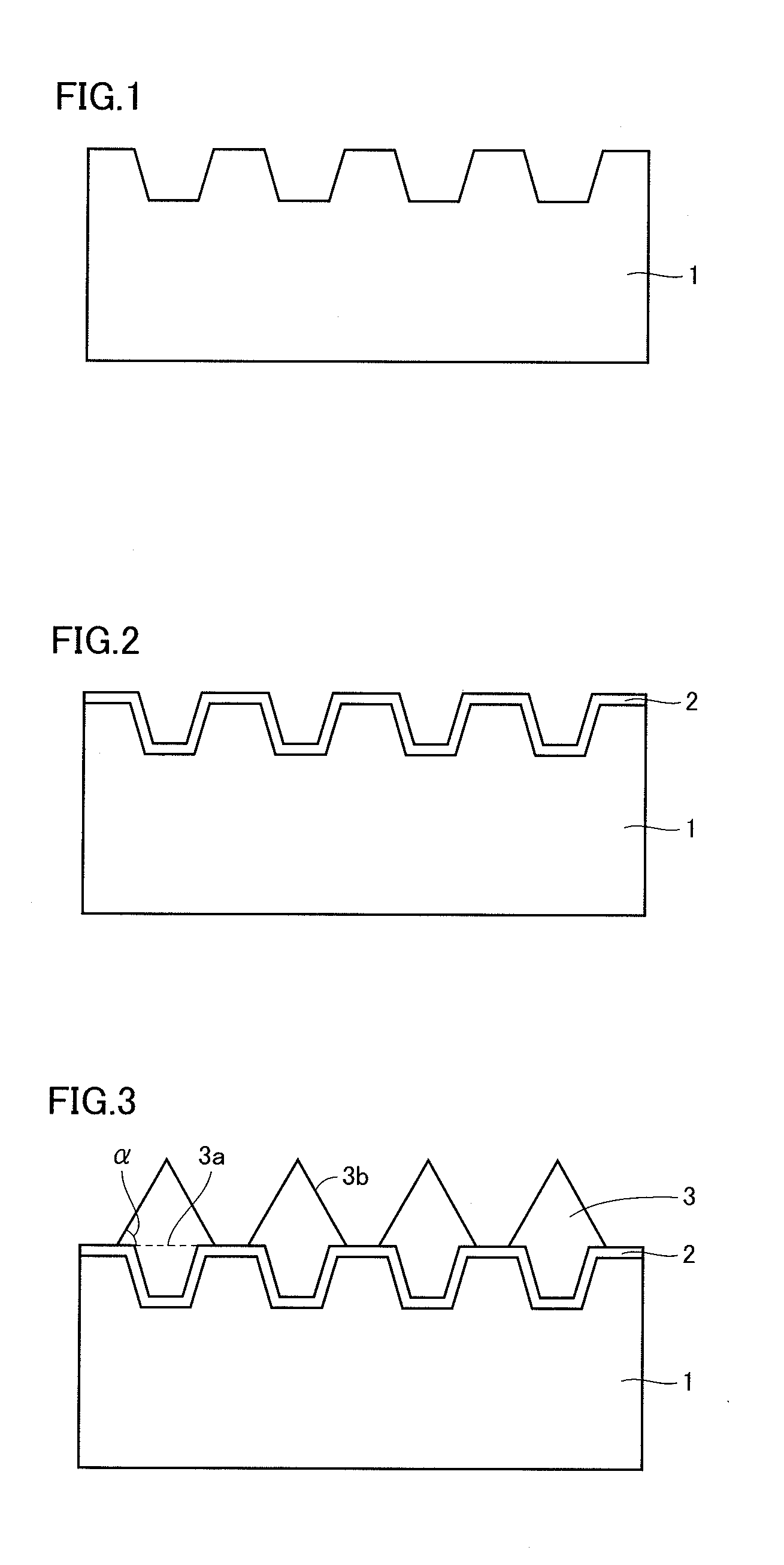
[0039]First, as shown in a schematic cross-sectional view of FIG. 1, a step of preparing a substrate 1 having concave and convex portions on its surface is performed. The step of preparing substrate 1 having concave and convex portions on its surface can be implemented, for example, by patterning a resist on the surface of substrate 1 which may be a sapphire substrate, a silicon carbide substrate, a gallium nitride substrate or a zinc oxide substrate, and etching a part of the surface of substrate 1 using ICP (Inductively Coupled Plasma) or the like.
[0040]Next, as shown in a schematic cross-sectional view of FIG. 2, a step of forming a buffer layer 2 on the surface of substrate 1 is performed. The step of forming buffer layer 2 can be implemented, for example, by laminating a nitride semiconductor layer made of a nitride semiconductor represented by an expression of Alx1Ga1-x1N (0≦x1≦1) on the surface of substrate 1 by sputtering. Preferably, an aluminum nitride layer is formed as b...
second embodiment
[0069]A second embodiment is characterized in that a nitride semiconductor laser device is fabricated rather than a nitride semiconductor light-emitting diode device.
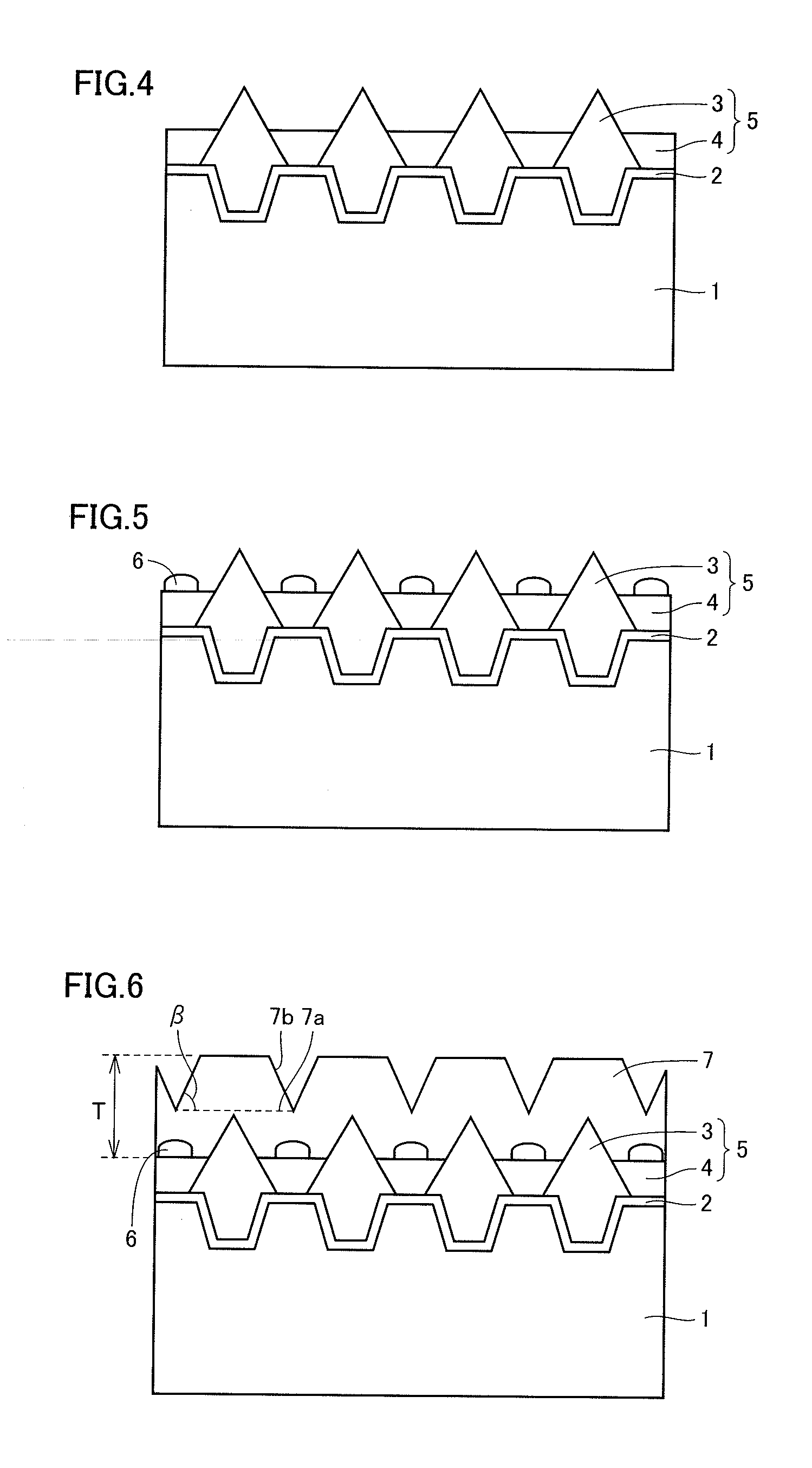
[0070]An example of a method of manufacturing the nitride semiconductor laser device in the second embodiment will be described below. First, in a manner similar to the first embodiment, buffer layer 2, inclined facet layers 3, first burying layer 4, silicon nitride layers 6, second nitride semiconductor layer 7 and third nitride semiconductor layer 8 are successively laminated on the surface of substrate 1.
[0071]Next, as shown in a schematic cross-sectional view of FIG. 11, an n type nitride semiconductor cladding layer 21, an n type nitride semiconductor light guide layer 22, a nitride semiconductor active layer 23, a nitride semiconductor protection layer 24, a p type nitride semiconductor light guide layer 25, a p type nitride semiconductor cladding layer 26 and a p type nitride semiconductor contact layer 27 are su...
third embodiment
[0084]A third embodiment is characterized in that a nitride semiconductor transistor device which is an example of electronic devices is fabricated, rather than light-emitting devices such as a nitride semiconductor light-emitting diode device and a nitride semiconductor laser device.
[0085]An example of a method of manufacturing the nitride semiconductor transistor device in the third embodiment will be described below. First, in a manner similar to the first and second embodiments, buffer layer 2, inclined facet layers 3, first burying layer 4, silicon nitride layers 6, second nitride semiconductor layer 7 and third nitride semiconductor layer 8 are successively laminated on the surface of substrate 1.
[0086]Next, as shown in a schematic cross-sectional view of FIG. 14, MOCVD is used to laminate a nitride semiconductor electron transit layer 31 made of undoped GaN or the like on upper surface 8a of third nitride semiconductor layer 8, and to laminate an n type nitride semiconductor ...
PUM
| Property | Measurement | Unit |
|---|---|---|
| angle | aaaaa | aaaaa |
| thickness | aaaaa | aaaaa |
| thickness | aaaaa | aaaaa |
Abstract
Description
Claims
Application Information