Differential sense amplifier circuit and method triggered by a clock signal through a switch circuit

a switch circuit and amplifier technology, applied in the field of integrated circuits, can solve the problems of generating kickback noise at input, sensitivity to noise, and speed limitation by slew rate, and achieve the effect of increasing the speed of regeneration and stable amplification

Inactive Publication Date: 2007-05-24
MACRONIX INT CO LTD
View PDF13 Cites 17 Cited by
  • Summary
  • Abstract
  • Description
  • Claims
  • Application Information

AI Technical Summary

Benefits of technology

[0010] Advantageously, the present invention comprises differential inputs, a latch circuit, and a pair of diode-connected transistors that provide stable amplification. Moreover, the present invention advantageously amplifies a differential input signal before a latch is enabled. Furthermore, the present invention advantageously increases the speed of regeneration with a positive feedback circuit.

Problems solved by technology

Problems associated with prior art sense amplifiers include sensitivity to noise, the speed is limited by slew rate, and a kickback noise is generated at input during the transitioning from low to high in a clock signal.

Method used


Image

  • Differential sense amplifier circuit and method triggered by a clock signal through a switch circuit
  • Differential sense amplifier circuit and method triggered by a clock signal through a switch circuit
  • Differential sense amplifier circuit and method triggered by a clock signal through a switch circuit

Examples


first embodiment

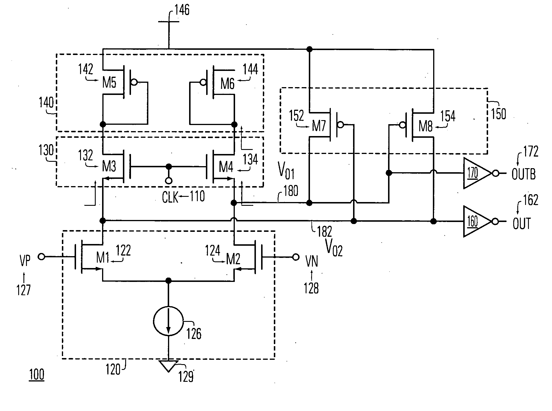
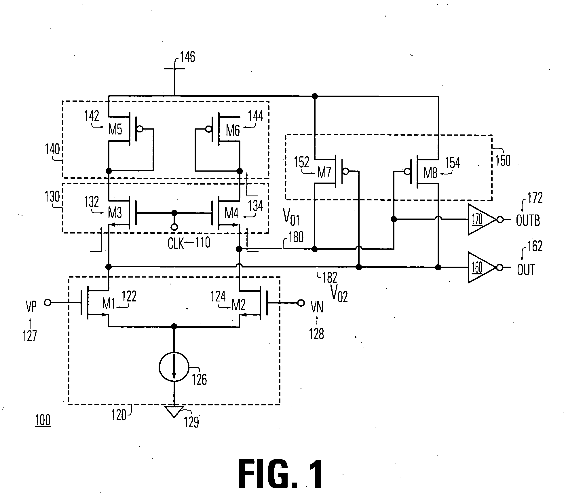
[0026] In FIG. 3, there is shown a circuit diagram illustrating the loop gain in the differential sense amplifier 100 in the first embodiment that functions as the preamplifier when the clock signal is set to the first signal level. In this configuration, when the clock signal is set to the first signal level, the M3 transistor 132 and the M4134 transistor are turned on, which also turn on the M5142 transistor and the M6144 transistor. The loop gain for the differential sense amplifier 100 that functions as an preamplifier can be calculated as follows:

Aloop=gm8[(ro3+ro5) / / (ro1 / / ro8)]*gm7*[(ro4+ro6) / / (ro2 / / ro7)]≈gm8*[ro2+ro5]*gm7*[(ro4+ro6)]ro1 / / ro8)>>(ro3+ro5); (ro2 / / ro7)>>(ro4+ro6) ∵gm8*[ro3+ro5]=gm7*[(ro4+ro6)]∵ro4=1 / gm4; ro6=1 / gm6

∴ The equation conforms to gm7*(ro4+ro6)32 >gm7*(1 / gm4+1 / gm6)<1

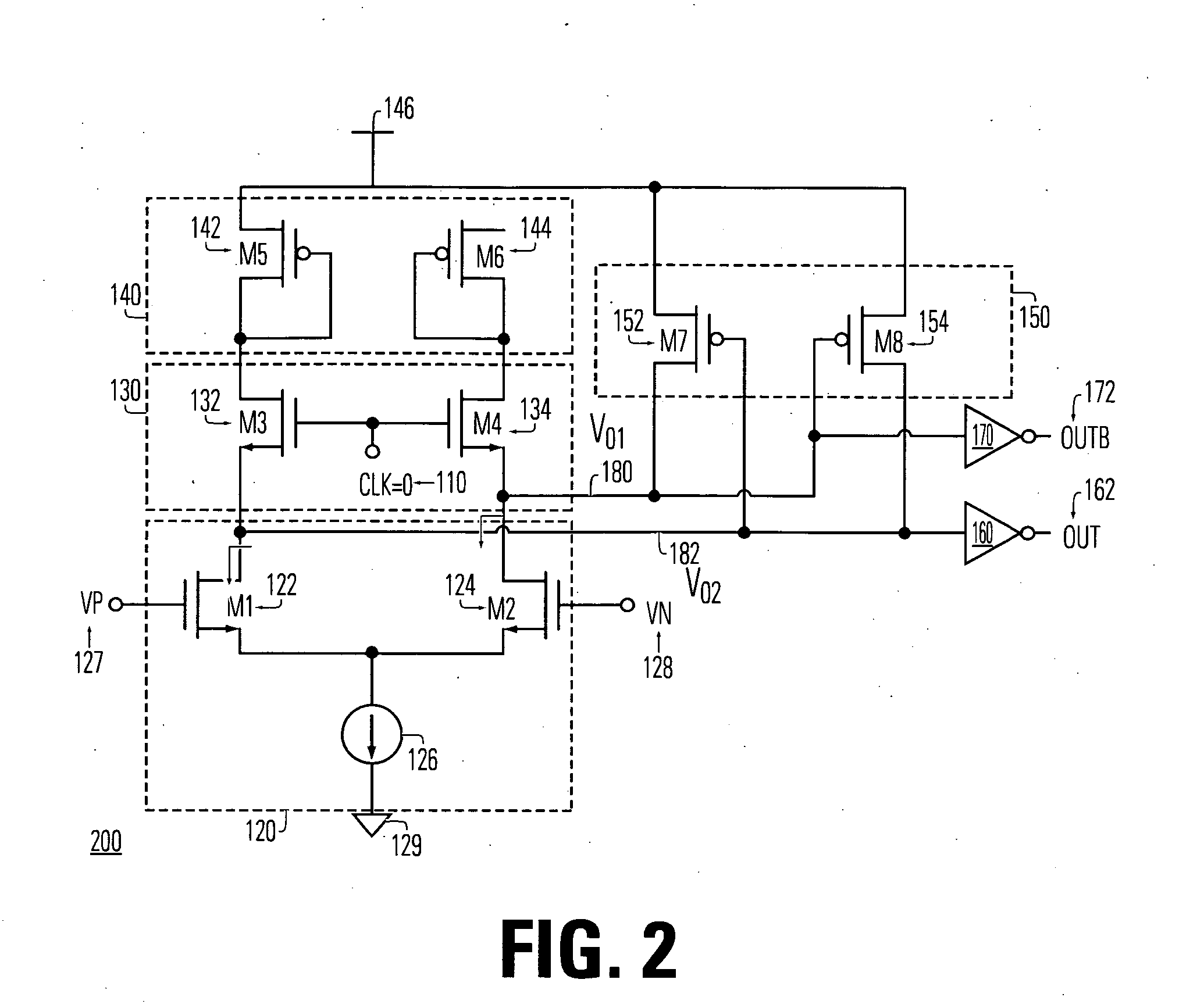
[0027]FIG. 4 is a circuit diagram illustrating the loop gain in the differential amplifier 200 in the first embodiment that functions as the latch circuit when the clock signal is set to t...

second embodiment

[0028] Turning now to FIG. 5, there is shown a circuit diagram illustrating a differential sense amplifier 500 that functions as a preamplifier when the clock signal is set to the first signal level and that functions as a latch circuit when the clock signal is set to the second signal level. In this embodiment, the differential sense amplifier 500 is designed with a R1 resistor 510 connected between the M3 transistor 132 and the Vdd voltage 146, replacing the M5142 transistor. A R2 resistor 520 is connected between the M4 transistor 134 and the Vdd voltage 146, replacing the M6144 transistor. In this embodiment, the differential sense amplifier 500 with the R1 resistor 510 and the R2 resistor 520 provides a larger input common mode range relative to the differential sense amplifier 100 as described in FIG. 1.

third embodiment

[0029] As shown in FIG. 6, there is a circuit diagram illustrating a differential sense amplifier 600 that functions as a preamplifier when the clock signal is set at the first signal level and that functions as a latch when the clock signal is set at the second signal level. The PMOS transistors 142 and 144 in FIG. 1 are replaced with NMOS transistors to generate the configuration in FIG. 6. The differential sense amplifier 600 comprises a pair of diode-connected transistors 610, the switch circuit 130, a differential amplifier 620, a positive feedback circuit 630, a first output inverter 640 and a second output inverter 650. The switch 130 includes the M3 transistor 132 and the M4 transistor 134 that are coupled, respectively, to the pair of diode-connected M5 transistor 612 and M6 transistor 614 on the lower side, and the differential pair 620 on the upper side. The positive feedback circuit 630 includes a M7 transistor 632 and a M8 transistor 634 that provide a positive feedback...


PUM


Abstract

A differential sense amplifier is described that can be configured as a preamplifier or a latch circuit as triggered by a clock signal connected to a switch circuit. When the clock signal is set at a first signal level, the switch circuit in the differential sense amplifier is activated so that the differential sense amplifier is configured as a preamplifier with a positive feedback circuit. When the clock signal is set at a second signal level, the switch circuit in the differential sense amplifier is deactivated so that the differential sense amplifier is configured as the latch circuit. For one read cycle, the differential sense amplifier operates first as the preamplifier and then as the latch circuit.

Description

BACKGROUND OF THE INVENTION [0001] 1. Field of the Invention [0002] The present invention relates generally to integrated circuits and more particularly to differential sense amplifiers that functions as a preamplifier and a latch circuit. [0003] 2. Description of Related Art [0004] Sense amplifiers are typically used to read the state (“0” or “1”) of memory cells in memory arrays, such as read-only memory (ROM) arrays. A ROM array may contain millions of memory cells arranged in rows and columns. The sources of each cell in a column may be connected to a source-column line, and the source-column line for a selected cell may be connected to a reference potential or ground during reading of the selected cell by a sense amplifier. The drains of each cell in a column are connected to a separate bit-line (drain-column line), and the drain-column line for a selected cell is connected to the input of the sense amplifier during reading of the selected cell. The control gates of each cell i...

Claims


Application Information

Patent Timeline
Patent Type & Authority Applications(United States)
IPC IPC(8): G01R19/00
CPCG11C7/02G11C7/062G11C7/065G11C7/1051G11C7/106
Inventor HSU, JER HAOWANG, TEIN YEN
Owner MACRONIX INT CO LTD
Why Eureka
Try Eureka