Electrochemical cell structure and method of fabrication

a technology of electrochemical cells and fabrication methods, applied in the field of electrochemical cells, can solve the problems of further alignment difficulties, difficult alignment of tools with previously defined structures on the substrate, and difficulty in accurate alignment, etc., and achieve the effect of high mass production and low cos

a technology of electrochemical cells and fabrication methods, applied in the field of electrochemical cells, can solve the problems of further alignment difficulties, difficult alignment of tools with previously defined structures on the substrate, and difficulty in accurate alignment, etc., and achieve the effect of high mass production and low cos

US20070122927A1Inactive Publication Date: 2007-05-31SEIKO EPSON CORP

Image

  • Electrochemical cell structure and method of fabrication
  • Electrochemical cell structure and method of fabrication
  • Electrochemical cell structure and method of fabrication

Examples


Embodiment Construction

[0015] Throughout the following description, like reference numerals identify like parts.

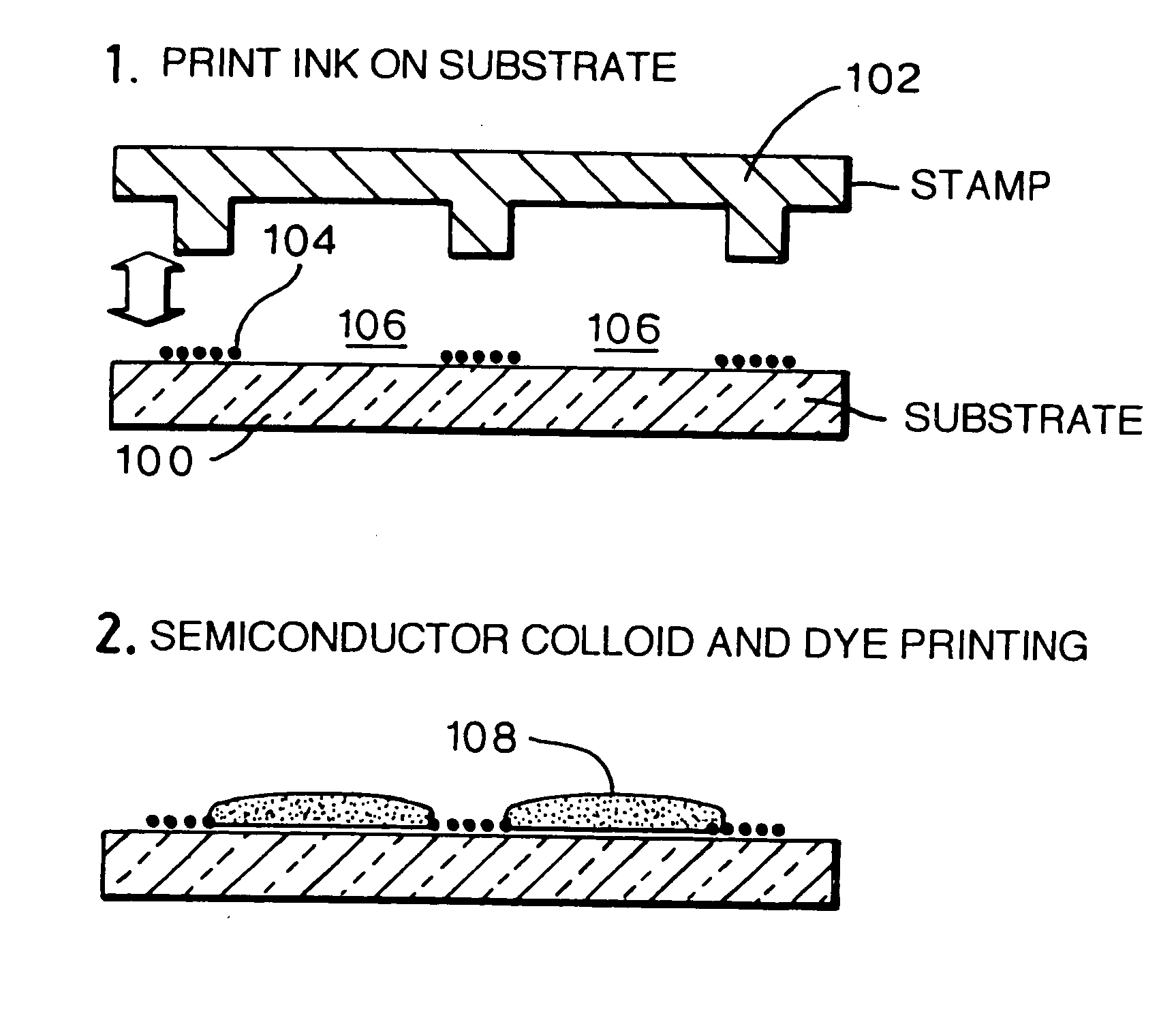
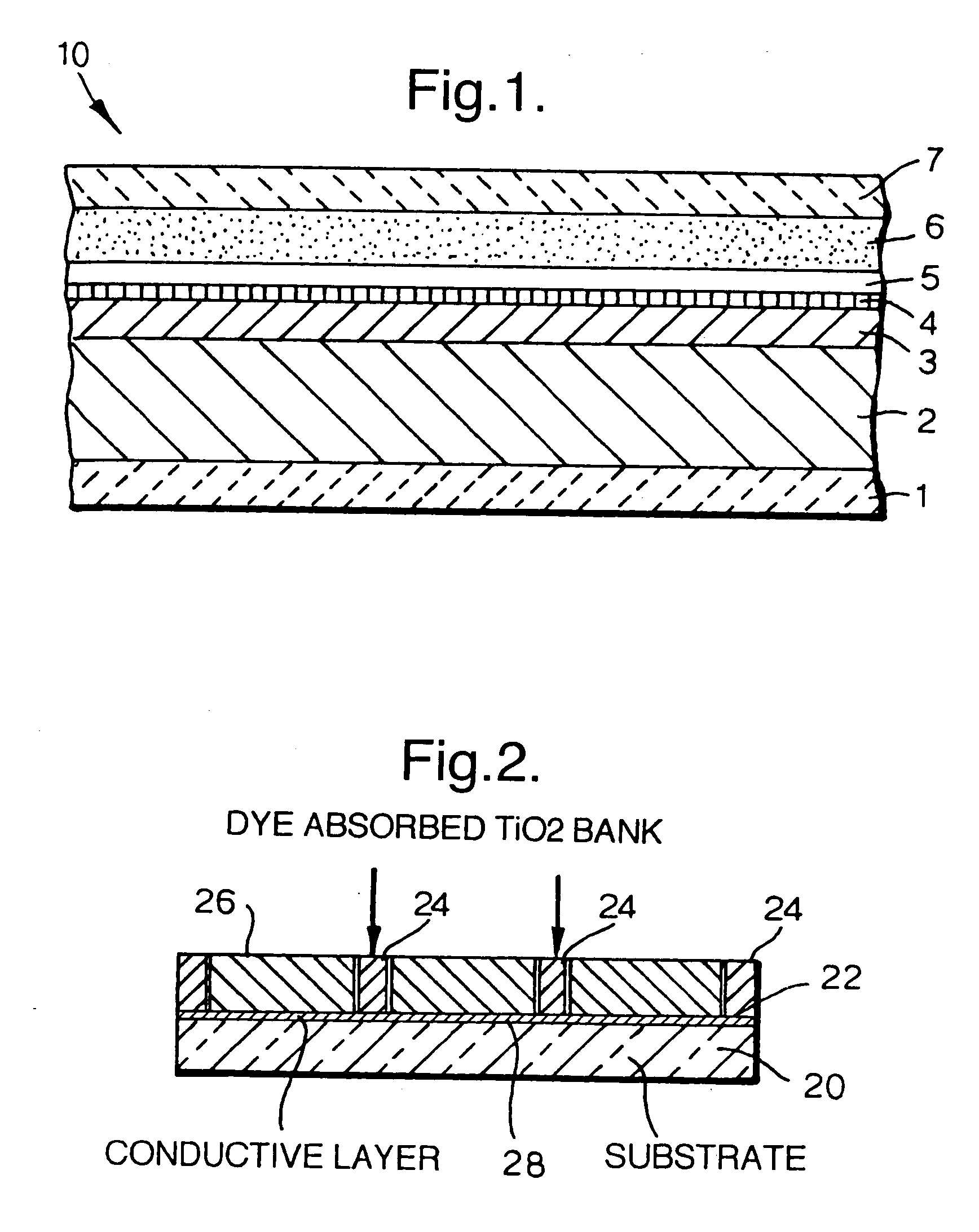
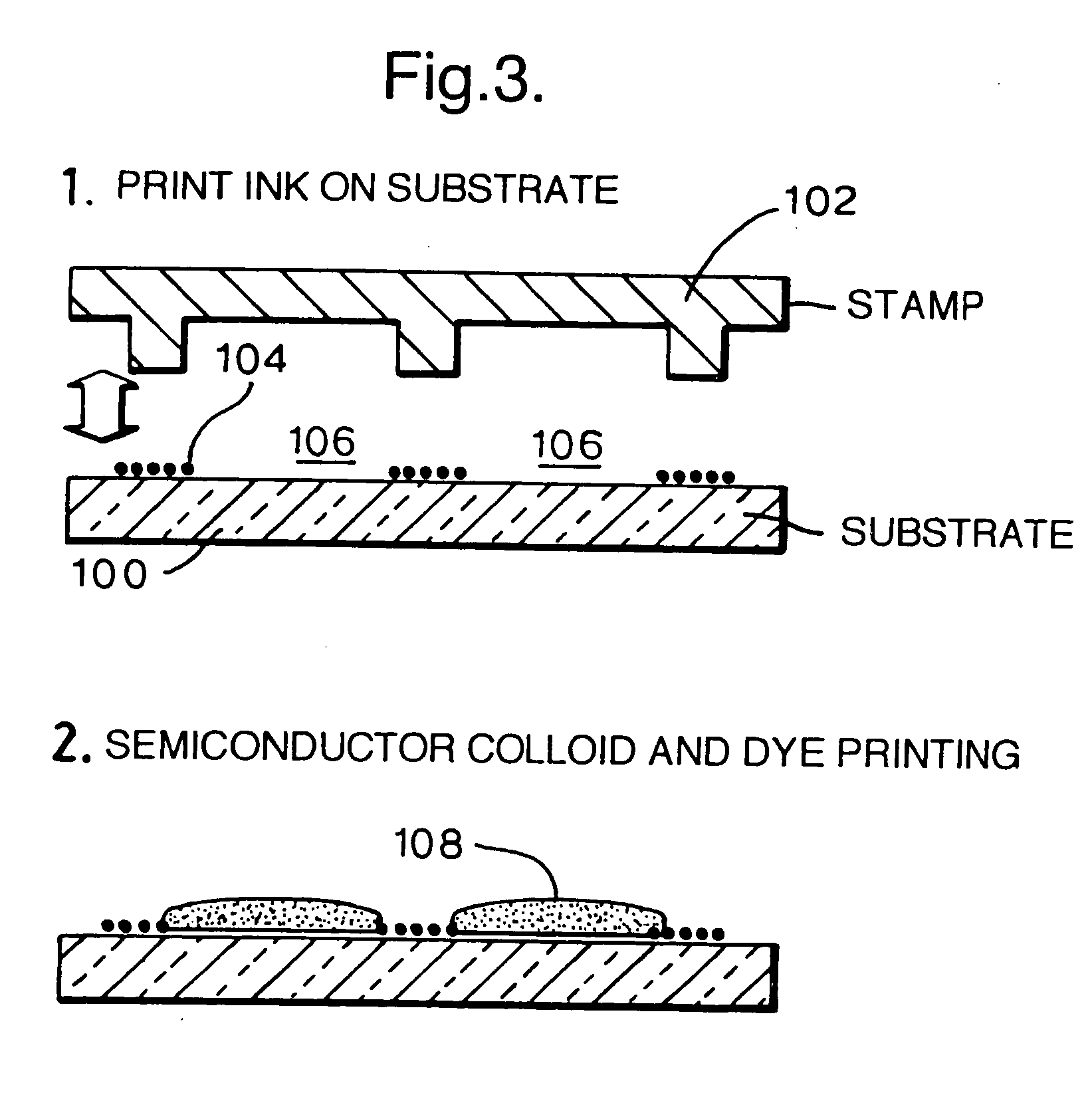
[0016]FIG. 2 illustrates a portion of a Dye-Sensitized Solar Cell (DSSC) having an array of pixel cells 28. The DSSC comprises a substrate wafer 20 having a conductive first electrode layer 22 deposited thereon. The pixel array structure 28 is created by way of a bank structure 24 formed on the first electrode layer 22 prior to the application of a metal oxide layer 26. A patterned metal oxide layer 26 is subsequently formed by inkjet printing the metal oxide 26 into each pixel cell 28 to form an array of micro-scale, high density pixel cells 28 surrounded by the banks 24 such that no metal oxide bridges the bank structure 24. Finally, a functional dye layer is formed on the metal oxide layer 26.

[0017] Preferred embodiments of the present invention for the formation of pixel array structures or the like will now be described.

[0018] A method of fabricating a pixel array structure according to ...


PUM


Abstract

One limitation to the realisation of mass produced electrochemical cells is a lack of high resolution patterning techniques providing accurate-alignment. Accordingly a method of fabricating a patterned structure in the manufacture of an electrochemical cell comprising a soft-contact printing and ink-jet printing is provided.

Description

FIELD OF THE INVENTION [0001] The present invention relates, in general, to an electrochemical cell and its method of manufacture. In particular, the present invention relates to the fabrication of a pixel array structure for a Dye-Sensitized Solar Cell (DSSC) using surface energy patterns that are defined by soft-contact printing. BACKGROUND OF THE INVENTION [0002] A Dye-Sensitized Solar Cell (DSSC) functions as an electrochemical cell. U.S. Pat. No. 4,927,721 entitled “Photo-Electrochemical Cell”, by M. Gratzel et al., discloses a typical DSSC. As illustrated in FIG. 1: a typical DSSC 10 comprises; a substrate 1; a first transparent electrode 2; a metal oxide layer 3; a functional dye layer 4; an electrolyte layer 5: a second electrode 6; and a second substrate 7. [0003] The DSSC 10 generates charge by the direct absorption of visible light. Since most metal oxides absorb light predominantly in the ultra-violet region of the electromagnetic spectrum, the functional dye 4 is absorb...

Claims


Application Information

Patent Timeline
31 May 2007
Publication
US20070122927A1
IPC
H01L21/00
CPC
B82Y30/00; H01G9/2031; H01G9/2068; H01L51/0004; Y02E10/542; Y02P70/50; H10K71/13; H01G9/2059
Inventors
LI, SHUNPU; ISHIDA, MASAYA