Nanoscale Sensor

a sensor and nano-scale technology, applied in the field of nano-scale sensors, can solve the problems of increasing the size of the sensor, limiting the life span, and causing the failure of structures and engineering materials, and achieve the effect of high reliability

Inactive Publication Date: 2007-06-07
PHYSICAL LOGIC
View PDF25 Cites 50 Cited by
  • Summary
  • Abstract
  • Description
  • Claims
  • Application Information

AI Technical Summary

Benefits of technology

[0005] In order to detect the smallest movements or vibrations it would be desirable to have a sensor having a functional element that is nano sized, yet wherein the changes in the sensor properties would be readily measurable on a macrosc

Problems solved by technology

The current generation of such sensors needs power, which increases their size and limits the

Method used


Image

  • Nanoscale Sensor
  • Nanoscale Sensor
  • Nanoscale Sensor

Examples


Embodiment Construction

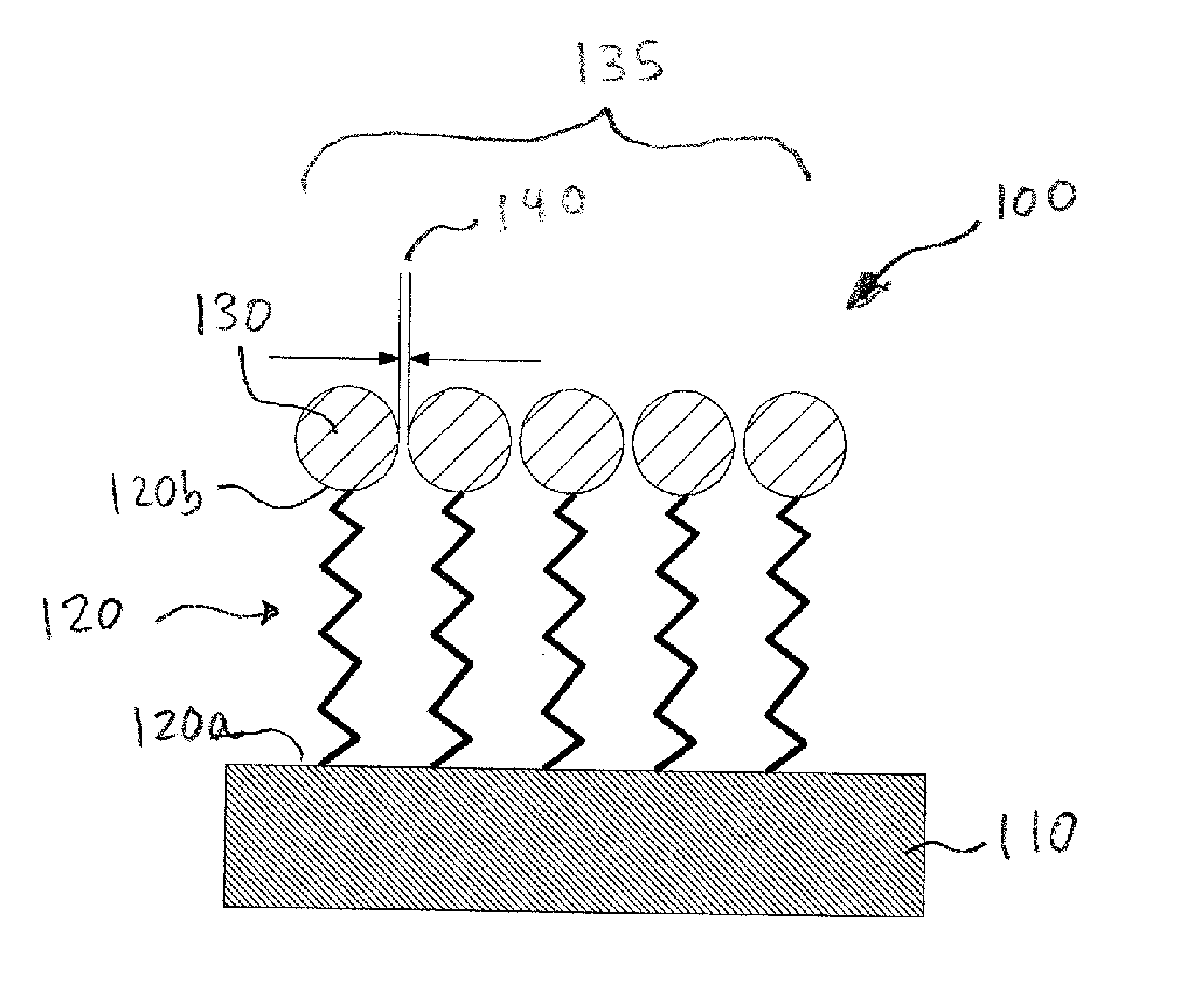
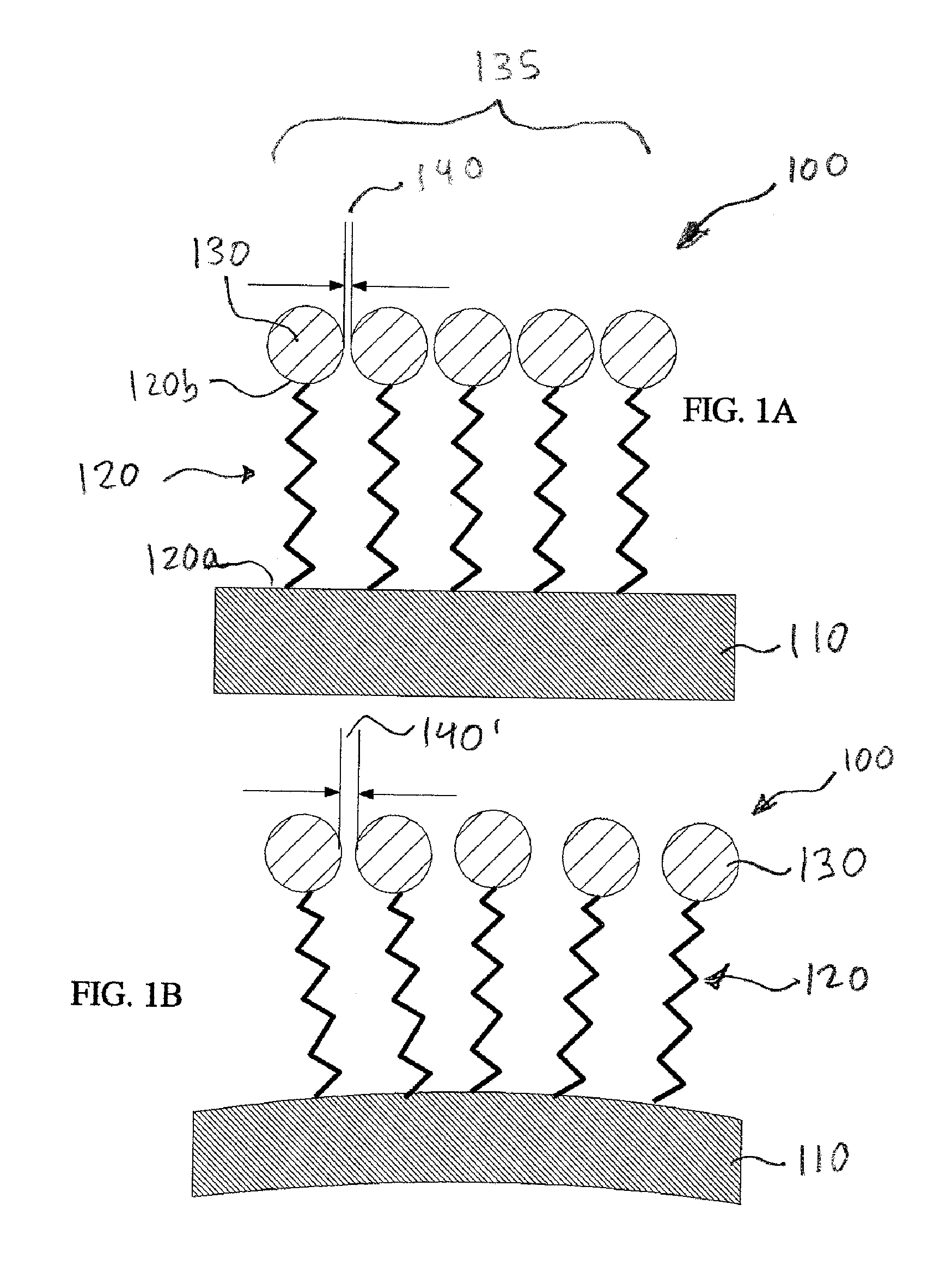
[0027] Referring to FIGS. 1 through 15, wherein like reference numerals refer to like components in the various views, there is illustrated therein a new and improved sensor, generally denominated 100 herein.

[0028] In accordance with the present invention, a nanoscale device is constructed on a non-rigid substrate 110. As shown in FIG. 1A, various long chain molecules 120 or high aspect ratio molecular assemblies are attached at one end 120a to the non-rigid substrate to extend upward from the substrate to form a dielectric or non electrically conductive column. On the other end of the column 120b is attached substantially equiaxed particles 130. The column distribution on the substrate is adjusted relative to the dimensions of the substrate to form a densely packed array of particle 135 such that the columns 120 act as spacers separating the particle 130 in the array 135 away from the substrate. Depending on the spacing and size of the molecular species that forms columns 120 and ...


PUM


Abstract

A plurality of densely packed nano-particles are arrayed on a elastic substrate via an intervening spacer by a combination of self-assembly methods or imprinting. The coated substrate is useful as a sensor device as the substrate is sufficiently non-rigid such that the deformation increases the separation between nano-particles resulting in a measurable change in the physical properties of the array. When the array comprises of closely packed conductive nano-particles deformation of the substrate disturbs the electrical continuity between the particles resulting in a significant increase in resistivity. The various optical properties of the device may exhibit measurable changes depending on the size and composition of the nano-particles, as well as the means for attaching them to the substrate.

Description

CROSS REFERENCE TO RELATED APPLICATIONS [0001] The present application claims priority to the U.S. provisional application having Ser. No. 60 / 738,927 entitled “Nanoparticle Vibration and Acceleration Sensors”, filed on Nov. 21, 2006 which is incorporated herein by reference. The present application also claims priority to the U.S. provisional application having Ser. No. 60 / 738,793 entitled “Nanoscale Sensor”, filed on Nov. 21, 2006 which is incorporated herein by reference. The present application further claims priority to the U.S. provisional application having Ser. No. 60 / 738,778 entitled “Polymer Nanosensor Device”, filed on Nov. 21, 2006 which is incorporated herein by reference.BACKGROUND OF INVENTION [0002] The present invention relates to a composition of useful structures and configures therefore for forming sensors having an ultra-high sensitivity to acceleration, deformation, vibration and the like physical disturbances. [0003] Prior methods of sensing small mechanical mo...

Claims


Application Information

Patent Timeline
IPC IPC(8): G11B5/33G11B5/127
CPCB82Y5/00B82Y15/00B82Y30/00G01H11/06G01N33/54373G01P15/0802G01P15/0894G01P15/12G01P15/123G01P2015/0828
Inventor OFEK, ERANLICHTENSTEIN, AMIRAXELROD, NOEL
Owner PHYSICAL LOGIC
Why Eureka
Try Eureka