

Field effect transistor
a field effect transistor and transistor technology, applied in the field of field effect transistors, can solve the problems of increased specific on-state resistance and circuit breakage, and achieve the effect of low specific on-state resistance and high work function
- Summary
- Abstract
- Description
- Claims
- Application Information
AI Technical Summary
Benefits of technology
Problems solved by technology
Method used
Image

Examples
embodiment 1
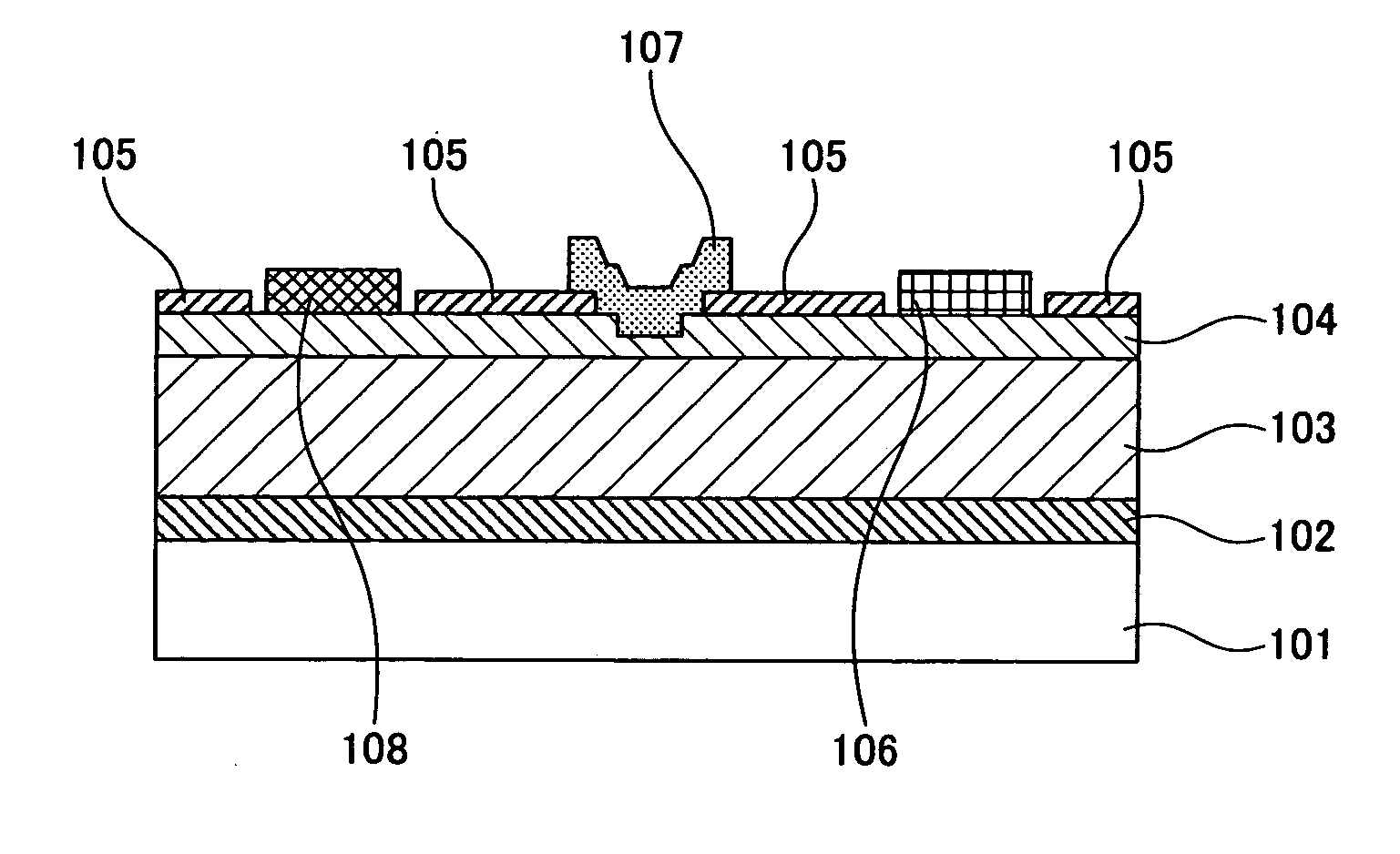
[0046]FIG. 1 is a sectional view showing a field effect transistor using a conductive oxide for a gate electrode according to Embodiment 1 of the present invention.
[0047] In FIG. 1, reference numeral 101 denotes a sapphire substrate, reference numeral 102 denotes an AlN buffer layer, reference numeral 103 denotes a first undoped GaN layer, reference numeral 104 denotes a first undoped AlGaN layer, reference numeral 105 denotes a SiO2 thin film, reference numeral 106 denotes a Ti / Al drain electrode, reference numeral 107 denotes a ZnInSnO gate electrode, and reference numeral 108 denotes a Ti / Al source electrode.
[0048]FIG. 1 shows the configuration of the field effect transistor of so-called normally-off type according to Embodiment 1. A threshold voltage VP is larger than 0 V. The feature of this configuration is the use of ZnInSnO for the gate electrode. In this configuration, the AlN buffer layer 102 having a thickness of 0.5 μm, the first undoped GaN layer 103 having a thicknes...
embodiment 2
[0059]FIG. 4 is a sectional view showing a field effect transistor using a conductive oxide for a gate electrode according to Embodiment 2 of the present invention.
[0060] In FIG. 4, reference numeral 401 denotes an n-type Si substrate, reference numeral 402 denotes an AlN buffer layer, reference numeral 403 denotes a first undoped GaN layer, reference numeral 404 denotes a first undoped AlGaN layer, reference numeral 405 denotes a Ti / Al drain electrode, reference numeral 406 denotes a ZnInSnO gate electrode, reference numeral 407 denotes a Ti / Al source electrode, reference numeral 408 denotes a Au wire, reference numeral 409 denotes a via hole, and reference numeral 410 denotes an Al backside source electrode.
[0061]FIG. 4 shows the configuration of the field effect transistor using the ZnInSnO gate electrode 406 according to Embodiment 2. In this configuration, the AlN buffer layer 402 having a thickness of 200 nm, the first undoped GaN layer 403 having a thickness of 1 μm, and th...
embodiment 3
[0066]FIG. 6 is a sectional view showing a field effect transistor using a conductive oxide for a gate electrode according to Embodiment 3 of the present invention.
[0067] In FIG. 6, reference numeral 601 denotes a GaN substrate, reference numeral 602 denotes a first undoped GaN layer, reference numeral 603 denotes a first undoped AlGaN layer, reference numeral 604 denotes a Ti / Al drain electrode, reference numeral 605 denotes an AlGaNOx oxide layer, reference numeral 606 denotes a ZnInSnO gate electrode, and reference numeral 607 denotes a Ti / Al source electrode.
[0068]FIG. 6 shows the structure of the field effect transistor using ZnInSnO for the gate electrode according to Embodiment 3. In this structure, the first undoped GaN layer 602 having a thickness of 5 μm and the first undoped AlGaN layer having a thickness of 12 nm and are formed in this order on a plane (0001) of the GaN substrate 601. In this epitaxial layer, the composition ratio of the first undoped AlGaN layer 603 i...
PUM
 Abstract
Description
Claims
Application Information