System and method for common mode calibration in an analog to digital converter

a technology common mode, applied in the field of analog to digital converter, can solve the problems of reducing the gain, not a commensurate increase or decrease in the common mode voltage of the reference voltage, and achieve the effect of improving the gain of the analog-to-digital converter (adc) preamplifier

Active Publication Date: 2007-06-14
AVAGO TECH INT SALES PTE LTD
View PDF19 Cites 15 Cited by
  • Summary
  • Abstract
  • Description
  • Claims
  • Application Information

AI Technical Summary

Benefits of technology

[0006] In an embodiment, a method and apparatus is provided to improve a gain of an analog-to-digital converter (ADC) preamplifier. A conversion circuit calibrates the ADC by minimizing a common mode voltage offset between an input voltage and a reference voltage during the hold mode of a track and hold circuit.
[0011] The common mode voltage circuit is also coupled to the output of the second integrator. The common mode voltage circuit varies a common mode voltage of the front-end circuit to minimize the common mode voltage offset between an input common mode voltage and the common mode voltage of the calibration voltage. Minimizing the common mode voltage offset improves the gain of the ADC preamplifier and calibrates the ADC.
[0012] An exemplary method for improving the gain of the ADC preamplifier is executed during a hold phase of the track-and-hold circuit. The common mode voltage offset is captured in the hold mode for calibration because input data is sampled by the ADC in hold mode. Minimizing the common mode voltage offset in the hold phase can effectively improve ADC preamplifier gain and the ADC's overall performance. The front-end circuit is a track-and-hold circuit in this example. First, the feedback controller circuit senses the ADC output. The feedback controller circuit adjusts the calibration voltage to reduce the calibration offset voltage. Then, the feedback controller circuit calibrates the ADC. Calibration is performed by adjusting the input common mode voltage to minimize the common mode voltage offset. Minimizing the common mode voltage offset increases the gain of the ADC preamplifier.

Problems solved by technology

The gain decreases because the differential amplifier is biased at an un-balanced operation point due to the common mode voltage offset.
However, there is not a commensurate increase or decrease in the common mode voltage of the reference voltage.

Method used


Image

  • System and method for common mode calibration in an analog to digital converter
  • System and method for common mode calibration in an analog to digital converter
  • System and method for common mode calibration in an analog to digital converter

Examples


Embodiment Construction

Index

[0033] I. OVERVIEW

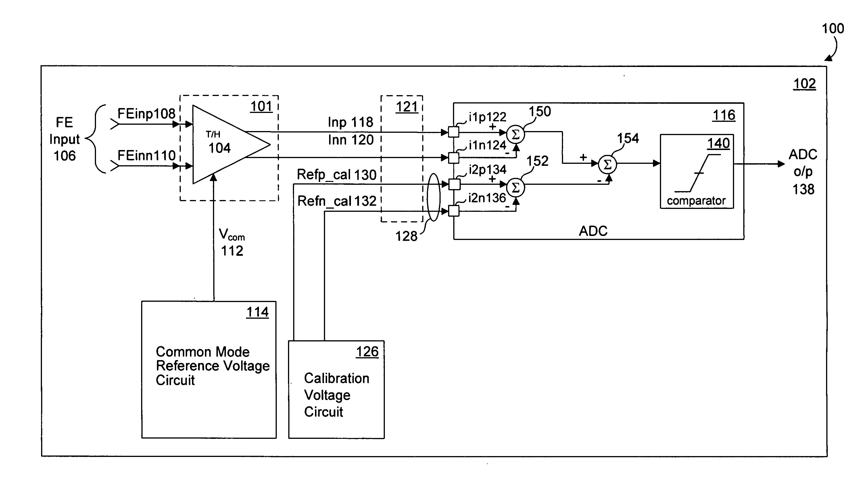
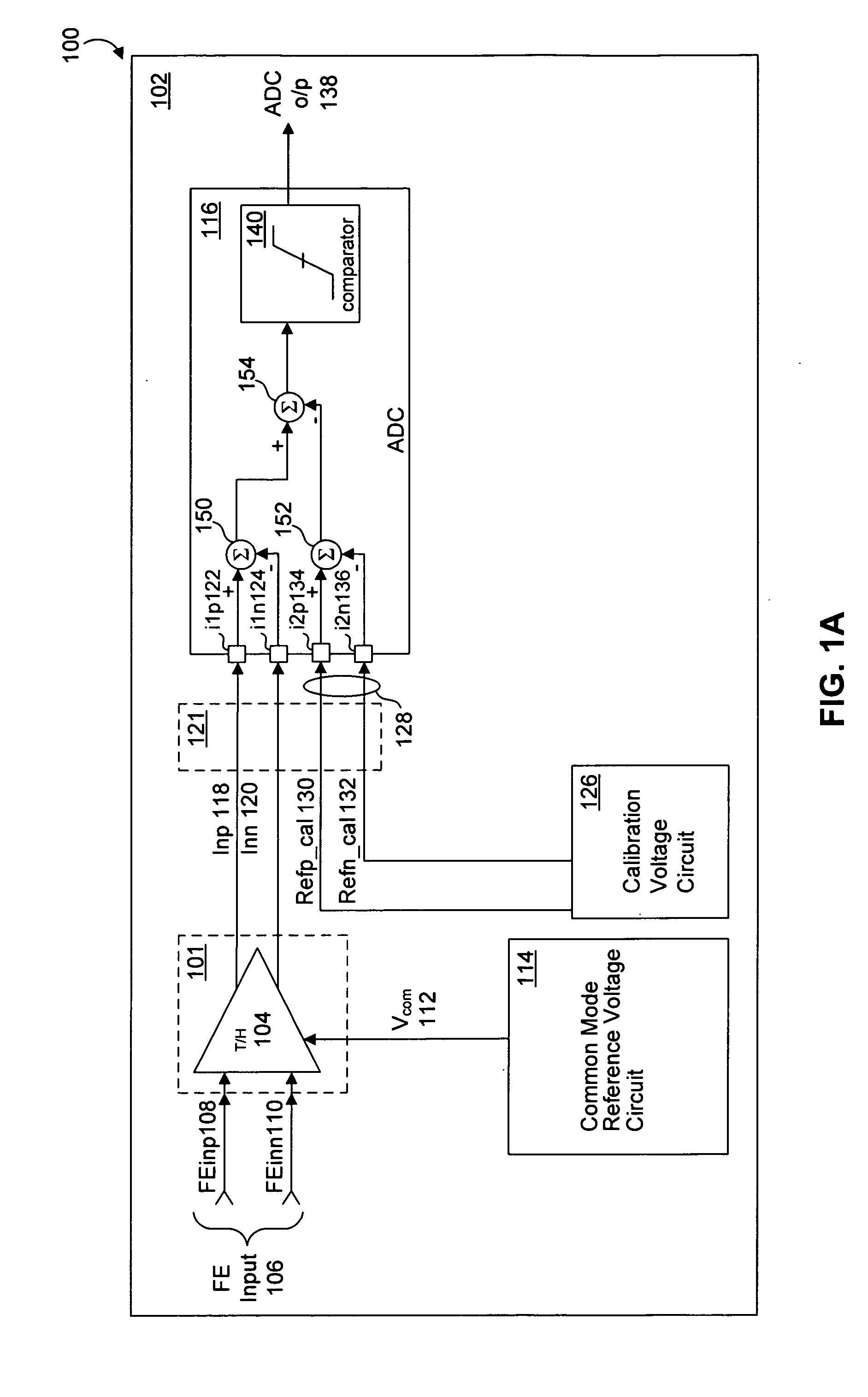
[0034] II. CONVERSION CIRCUIT

[0035] III. ADC CIRCUIT

[0036] IV. ADC NORMAL OPERATION MODE

[0037] V. ADC COMMON MODE CALIBRATION MODE

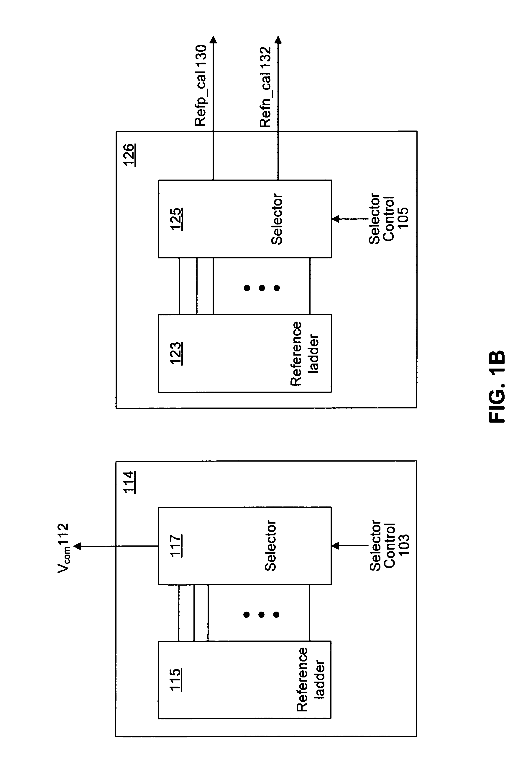
[0038] VI. ADC REFERENCE VOLTAGE CALIBRATION MODE

[0039] VII. ADC REFERENCE VOLTAGE CALIBRATION CIRCUIT

[0040] VIII. ADC COMMON MODE CALIBRATION CIRCUIT

[0041] IX. METHOD FOR COMMON MODE CALIBRATION

[0042] X. METHOD FOR INCREASING ADC INPUT PREAMPLIFIER GAIN

I. Overview

[0043] As introduced above, various embodiments of the invention involve an apparatus and / or method for common mode calibration in an analog to digital converter. FIGS. 1-10, described below, illustrate this approach.

[0044] This specification discloses one or more embodiments that incorporate the features of this invention. The disclosed embodiment(s) merely exemplify the invention. The scope of the invention is not limited to the disclosed embodiment(s). The invention is defined by the claims appended hereto.

[0045] The embodiment(s) described, and referenc...


PUM


Abstract

A conversion circuit increases a gain of an analog-to-digital converter (ADC) preamplifier by minimizing a common mode offset voltage between an input signal and a reference signal. The feedback controller circuit calibrates an input common mode voltage to mitigate a common mode offset voltage. Reduction of the common mode offset voltage increases the gain of the ADC preamplifier. In an example, the method is executed during a hold phase of a track-and-hold circuit that transmits the input signal to the ADC.

Description

CROSS REFERENCE TO RELATED APPLICATIONS [0001] This application claims the benefit of U.S. Provisional Application No. 60 / 750,064, filed Dec. 14, 2005, which is incorporated herein by reference in its entirety.FIELD OF THE INVENTION [0002] The present invention is generally directed to an analog to digital converter (ADC). More particularly, the invention relates to an apparatus and method for calibrating an ADC. BACKGROUND [0003] In an analog-to-digital converter (ADC), an input voltage having a common mode voltage is input to an ADC input preamplifier. A reference voltage having a common mode voltage is also applied to the ADC input preamplifier. The input preamplifier amplifies a common mode voltage offset between the ADC input voltage and the reference voltage. The common mode voltage of the ADC input voltage does not equal the common mode voltage of the reference voltage, therefore a gain of the ADC input preamplifier decreases. The gain decreases because the differential ampli...

Claims


Application Information

Patent Timeline
Patent Type & Authority Applications(United States)
IPC IPC(8): H03M1/12
CPCH03M1/0607H03M1/1019H03M1/34
Inventor CHEN, CHUN-YING
Owner AVAGO TECH INT SALES PTE LTD
Why Eureka
Try Eureka