

Liquid crystal display device and method of fabricating the same
a liquid crystal display and display panel technology, applied in static indicating devices, instruments, non-linear optics, etc., can solve the problems of increasing fabrication costs, waste of panel area around the edges of liquid crystal display panels, and inefficient use of panel area, so as to achieve low unit costs
- Summary
- Abstract
- Description
- Claims
- Application Information
AI Technical Summary
Benefits of technology
Problems solved by technology
Method used
Image

Examples
first embodiment
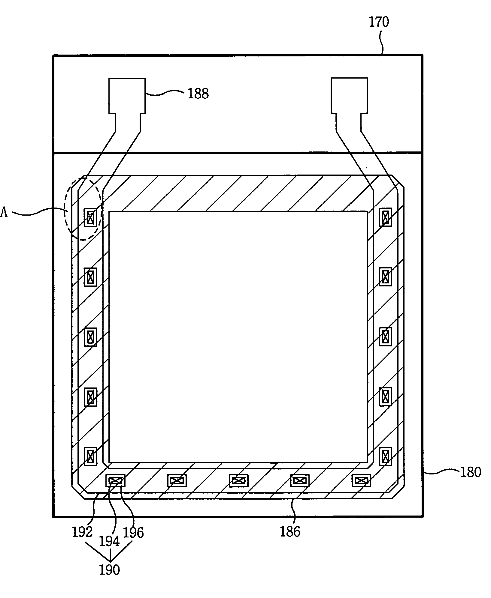
[0035]FIG. 3 is a plan view of a liquid crystal display panel according to the present invention. Referring to FIG. 3, the liquid crystal display panel includes a thin film transistor substrate 170 on which a thin film transistor array is formed; a color filter substrate 180 on which a color filter array is formed; and a conductive sealant 186 for bonding the thin film transistor substrate 170 and the color filter substrate 180 together. The thin film transistor array substrate 170 has a thin film transistor array formed on a lower substrate, and the thin film transistor array includes a gate line (not shown) and a data line (not shown) that are formed to cross each other; a thin film transistor (not shown) formed at the crossing of a gate line and a data line; a pixel electrode (not shown) connected to the thin film transistor; and a lower alignment film (not shown) on the pixel electrode for aligning liquid crystal.
[0036]FIG. 4 is a plan view of an enlarged A area in FIG. 3. FIG. ...
second embodiment
[0043]The reason why the gate driver is mounted directly on the panel in the present invention is to reduce the per unit cost of the liquid crystal display device and to simplify a module process. If the gate driver is directly mounted on the panel along with the formation of the gate line and the data line, the need for fabricating an integrated circuit of the gate driver separately and then adhering the integrated circuit to the panel part through a TCP is not necessary. Directly mounting the gate driver on the panel simplifies the connection process of the gate driver and reduces costs.
[0044]The liquid crystal display device according to the second embodiment of the present invention includes a thin film transistor substrate 270 on which a thin film transistor array is formed; a color filter substrate 280 on which a color filter array is formed; and a conductive sealant 186 for bonding the thin film transistor substrate 270 and the color filter substrate 280. The thin film transi...
third embodiment
[0062]The color filter array substrate 380 bonded to the thin film transistor array substrate 370 according to the foregoing third embodiment has a black matrix 384 for preventing light leakage; and a common electrode 382 for receiving the common voltage, on an upper substrate 311. Further, the color filter array substrate 380 includes an insulating pattern 350 in an area corresponding to the first and second connection patterns 325a and 325b of the thin film transistor array substrate 270. The insulating pattern 350 prevents a phenomenon in which a short circuit occurs between the common electrode 382 of the color filter array substrate 380 and the connection pattern 325a and 325b of the thin film transistor array substrate 370.
[0063]FIG. 12 is another cross-sectional view of a liquid crystal display device taken along line III-III′ shown in FIG. 10. When the color filter array substrate 380 and the thin film transistor array substrate 370 are bonded by the conductive sealant 186, ...
PUM
| Property | Measurement | Unit |
|---|---|---|
| conductive | aaaaa | aaaaa |
| insulating | aaaaa | aaaaa |
| light transmittance | aaaaa | aaaaa |
Abstract
Description
Claims
Application Information