Method for fabricating a probing pad of an integrated circuit chip
- Summary
- Abstract
- Description
- Claims
- Application Information
AI Technical Summary
Problems solved by technology
Method used
Image

Examples
Embodiment Construction
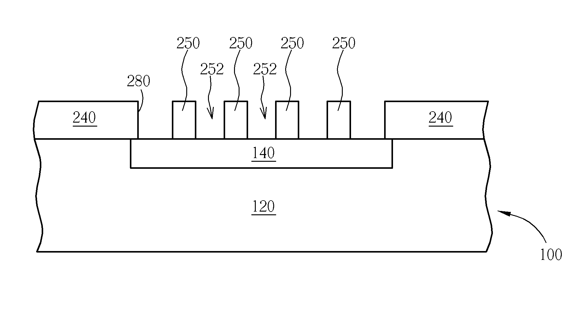
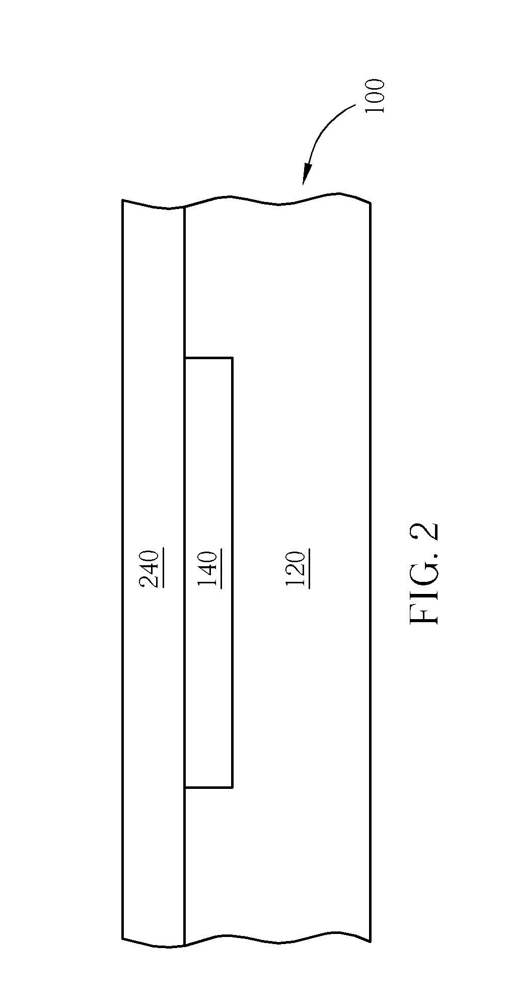
[0015] Please refer to FIGS. 2-6. FIGS. 2-6 are schematic, cross-sectional diagrams illustrating a method for fabricating a probing pad of an integrated circuit chip in accordance with one preferred embodiment of this invention. As shown in FIG. 2, a semiconductor integrated circuit chip 100 comprises thereon a base layer 120. It is understood that the base layer 120 may comprises various integrated circuit elements such as transistors, memory or logic devices and interconnection metal layers, which are not shown for the sake of simplicity.
[0016] A copper wiring layer 140 is embedded in the base layer 120. The copper wiring layer 140 may be surrounded by low dielectric constant materials, but not limited thereto. The copper wiring layer 140 has an exposed top surface.
[0017] The copper wiring layer 140 may be formed by etching a damascene trench into the base layer 120, then filling the damascene trench with copper, followed by chemical polishing the excess copper outside trench. A...
PUM
 Abstract
Description
Claims
Application Information
 - R&D Engineer
- R&D Manager
- IP Professional
- Industry Leading Data Capabilities
- Powerful AI technology
- Patent DNA Extraction
Browse by: Latest US Patents, China's latest patents, Technical Efficacy Thesaurus, Application Domain, Technology Topic.
© 2024 PatSnap. All rights reserved.Legal|Privacy policy|Modern Slavery Act Transparency Statement|Sitemap