Light emitting device package and method of manufacturing the same

a technology of light emitting devices and manufacturing methods, which is applied in the direction of basic electric elements, semiconductor devices, electrical apparatus, etc., can solve the problems of reducing the size of the structure of the led chip package, complex manufacturing process, and complex structure, and achieves the effect of simple structure and small siz

Inactive Publication Date: 2007-06-28
SAMSUNG DISPLAY CO LTD
View PDF5 Cites 30 Cited by
  • Summary
  • Abstract
  • Description
  • Claims
  • Application Information

AI Technical Summary

Benefits of technology

[0010]An exemplary aspect of the present invention provides a light emitting device package capable of

Problems solved by technology

In this conventional method of forming an LED, a complex structure is required for installing the LED chip, and the manufacturing process is also complicated.
Furthermore, an additional reflecting frame structure has to be formed for forming a reflecting surface on the periphery of the LED chip, and this may be an obstacle for reducing the size of the structure of the LED chip package.
Accordingly, it is very complicated and expensive to fabricate a conventional structure having a reflecting surface with a suitable surface roughness.
These processes may be a factor in increasing the manufac

Method used


Image

  • Light emitting device package and method of manufacturing the same
  • Light emitting device package and method of manufacturing the same
  • Light emitting device package and method of manufacturing the same

Examples


Embodiment Construction

[0030]Reference will now be made in detail to the exemplary embodiments of the present invention, examples of which are illustrated in the accompanying drawings, wherein like reference numerals refer to the like elements throughout. The exemplary embodiments are described below to explain the present invention by referring to the figures.

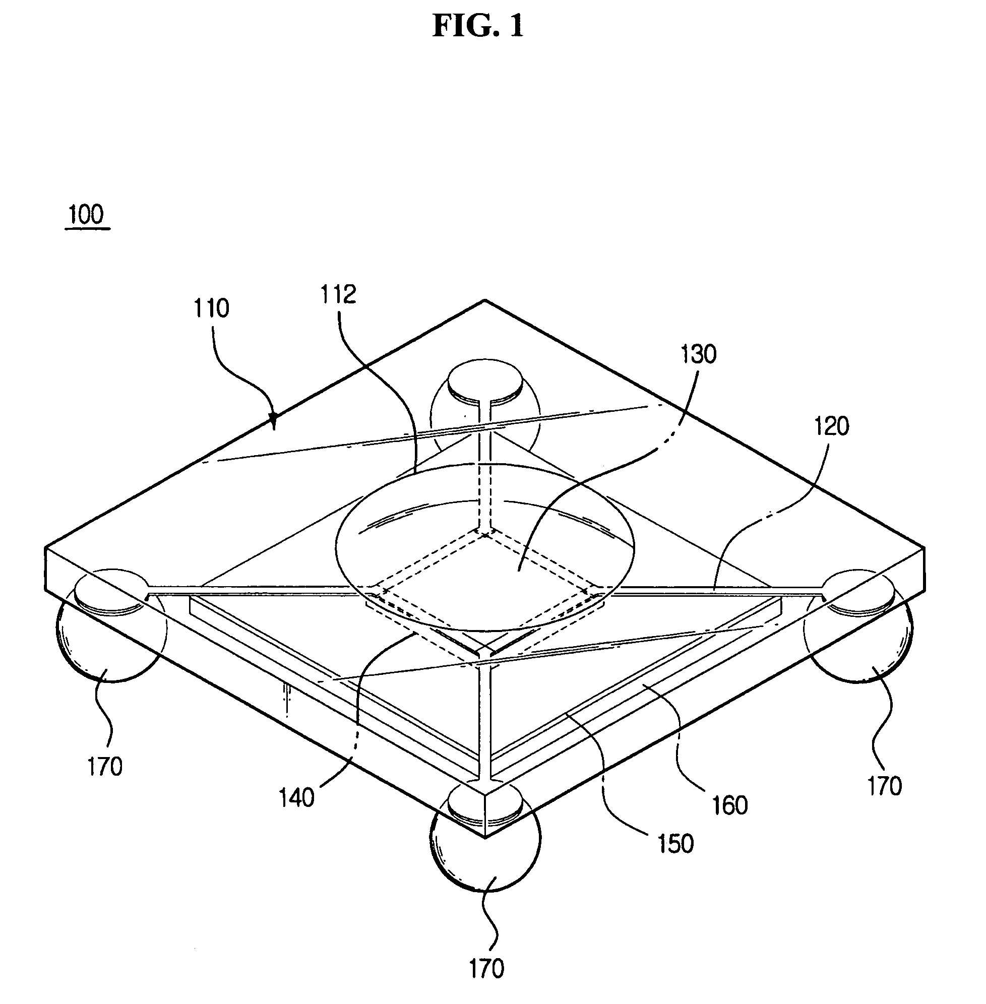
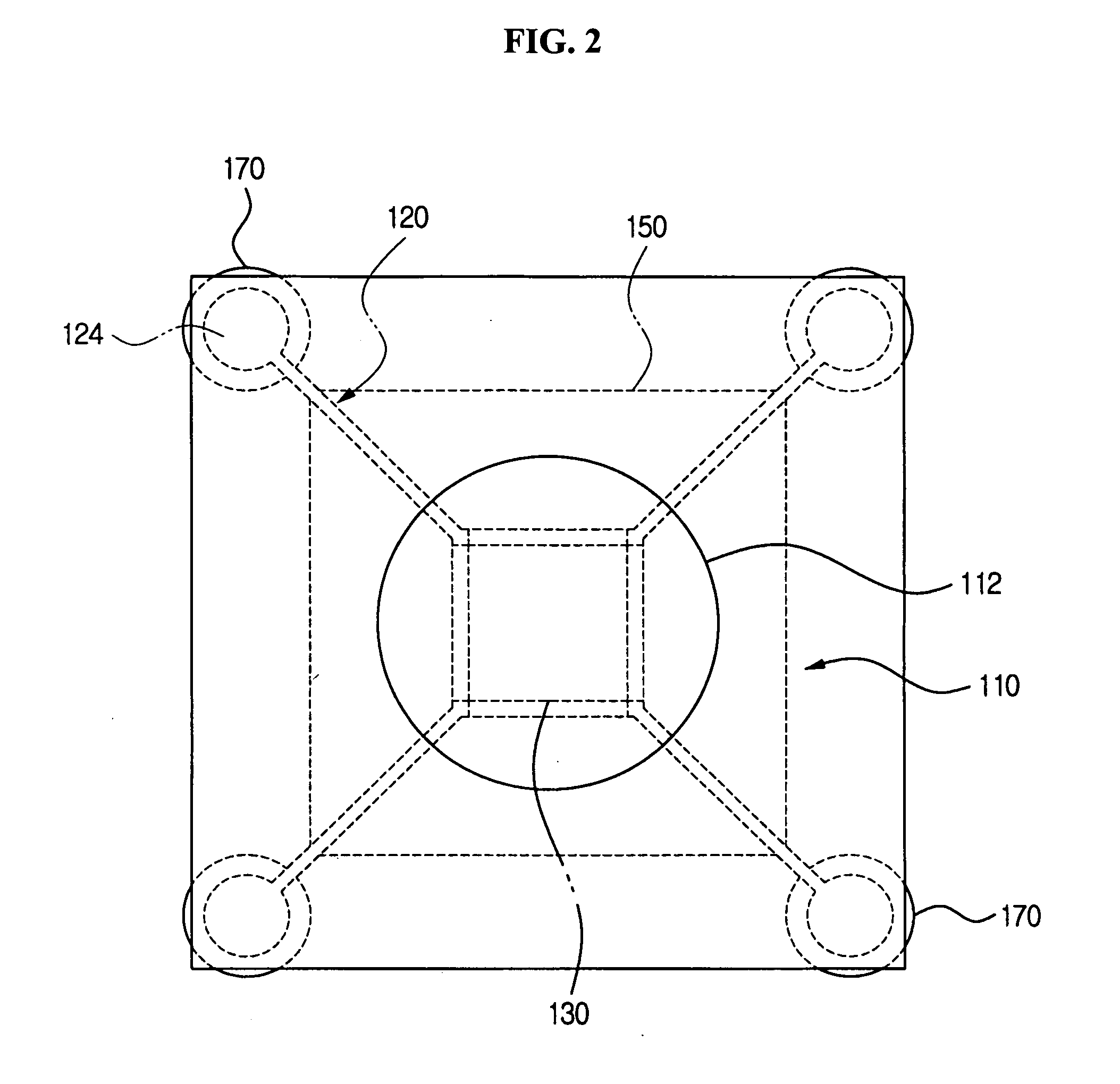
[0031]FIG. 1 is a perspective view illustrating a light emitting device package according to an exemplary embodiment of the present invention, FIG. 2 is a top view illustrating the light emitting device package of FIG. 1, and FIG. 3 is a cross-sectional view illustrating the light emitting device package of FIG. 1.

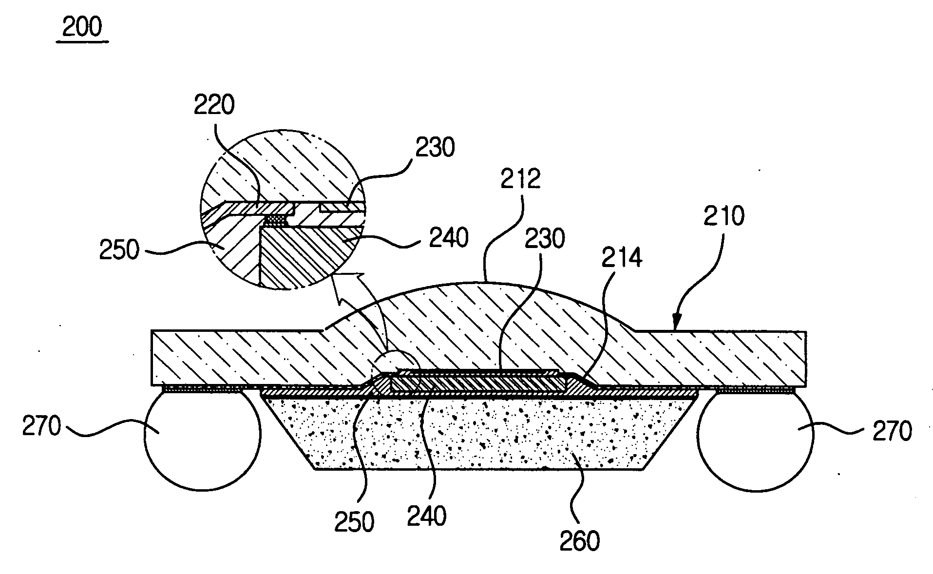
[0032]Referring to FIGS. 1 through 3, a light emitting device package 100 according to the present exemplary embodiment includes a transparent cover 110, a wavelength conversion layer 130, a light emitting device 140, an epoxy resin 150, a metal slug 160, and solder balls 170. Below the transparent cover 110, the wavelength conversion laye...


PUM


Abstract

A light emitting device package including a transparent cover having an electrode pattern formed on a bottom surface thereof; a light emitting device installed below the transparent cover and electrically connected to an external circuit via the electrode pattern; a fixing resin which fixes the light emitting device onto the bottom surface of the transparent cover; and a metal slug provided under the fixing resin to dissipate heat away from the light emitting device.

Description

CROSS-REFERENCE TO RELATED PATENT APPLICATIONS[0001]This application claims the benefit of Korean Patent Application No. 10-2005-130950, filed on Dec. 27, 2005, in the Korean Intellectual Property Office, the disclosure of which is incorporated herein by reference.BACKGROUND OF THE INVENTION[0002]1. Field of the Invention[0003]Apparatuses and methods consistent with the present invention relate to a light emitting device package that can be reduced in size and easily manufactured and a method of manufacturing the same.[0004]2. Description of the Related Art[0005]U.S. Pat. No. 6,599,768 discloses a “Surface Mounting Method for High Power Light Emitting Diode”. A substrate, formed of a material which readily transfers heat and electricity, is provided to be equipped with a high brightness light emitting diode. A trench is formed on the substrate and is filled with an insulating material to partition the substrate into two or more parts. A reflecting frame, including a reflecting surfa...

Claims


Application Information

Patent Timeline
IPC IPC(8): H01L33/00H01L33/48H01L33/62H01L33/64
CPCH01L25/0753H01L33/483H01L33/58H01L33/62H01L33/64H01L2224/16
Inventor DARBINIAN, ARTHURCHOI, SEUNG TAEKWON, KI HWANMOON, CHANG YOULSHIN, KYU HO
Owner SAMSUNG DISPLAY CO LTD
Why Eureka
Try Eureka