
Flicker detecting circuit and method in image sensor

a detection circuit and image sensor technology, applied in the field of semiconductor design techniques, can solve the problems of one-chip implementation, high power consumption, complex manufacturing process, etc., and achieve the effect of minimizing the implementation area and hardware resources of the semiconductor

Inactive Publication Date: 2007-06-28
INTELLECTUAL VENTURES II
View PDF9 Cites 33 Cited by
  • Summary
  • Abstract
  • Description
  • Claims
  • Application Information

AI Technical Summary

Benefits of technology

"The present invention provides a circuit and method for detecting flickers in an image sensor. The circuit and method extract luminance values from pixel data of two frames, calculate the difference between them, and detect flickers based on the distance between neighboring local minimum points. The technical effects of the invention are to minimize the semiconductor-implemented area and hardware resources needed for detecting flickers, while still accurately detecting them."

Problems solved by technology

The CCD has disadvantageously a complex driving method and a much power consumption.
Further, the CCD has the disadvantages that the manufacturing process is complicated because the number of masking processes is large and a one-chip implementation is difficult because a signal processing circuit cannot be built in a chip.
However, an analog signal introduced from a photo-receiving device, e.g., a photodiode, in the CMOS image sensor has diverse parasitic effects caused by a parasitic capacitance, a resistance, a dark current leakage, the inconsistency of features of a semiconductor device and so on.
Thus the noise acts as a critical factor for limiting a performance of the image sensor.
The cause that the noise occurs in the CMOS image sensor may be a kT / C noise related to a sampling of the image data, a 1 / f noise related to a circuit used for amplifying an image signal, and a Fixed Pattern Noise (FPN) related to the inconsistent signal processing circuits in the image sensor.
The FPN, among others, is visually very poor since it is seen in a vertical line or a strip form within the image and thus can easily be found by human eyes.
This method can obtain an exact flicker detective result but has a disadvantage that a hardware resource is wasted by the addition of the particular pixel array, and time and financial cost for designing and controlling the particular pixel array increase.

Method used


Image

  • Flicker detecting circuit and method in image sensor
  • Flicker detecting circuit and method in image sensor
  • Flicker detecting circuit and method in image sensor

Examples


Embodiment Construction

[0037] Hereinafter, the preferred embodiments of the present invention will be described with reference to the accompanying drawings. In the description and the drawings, the identical reference numerals refer to as the identical elements performing the same functions.

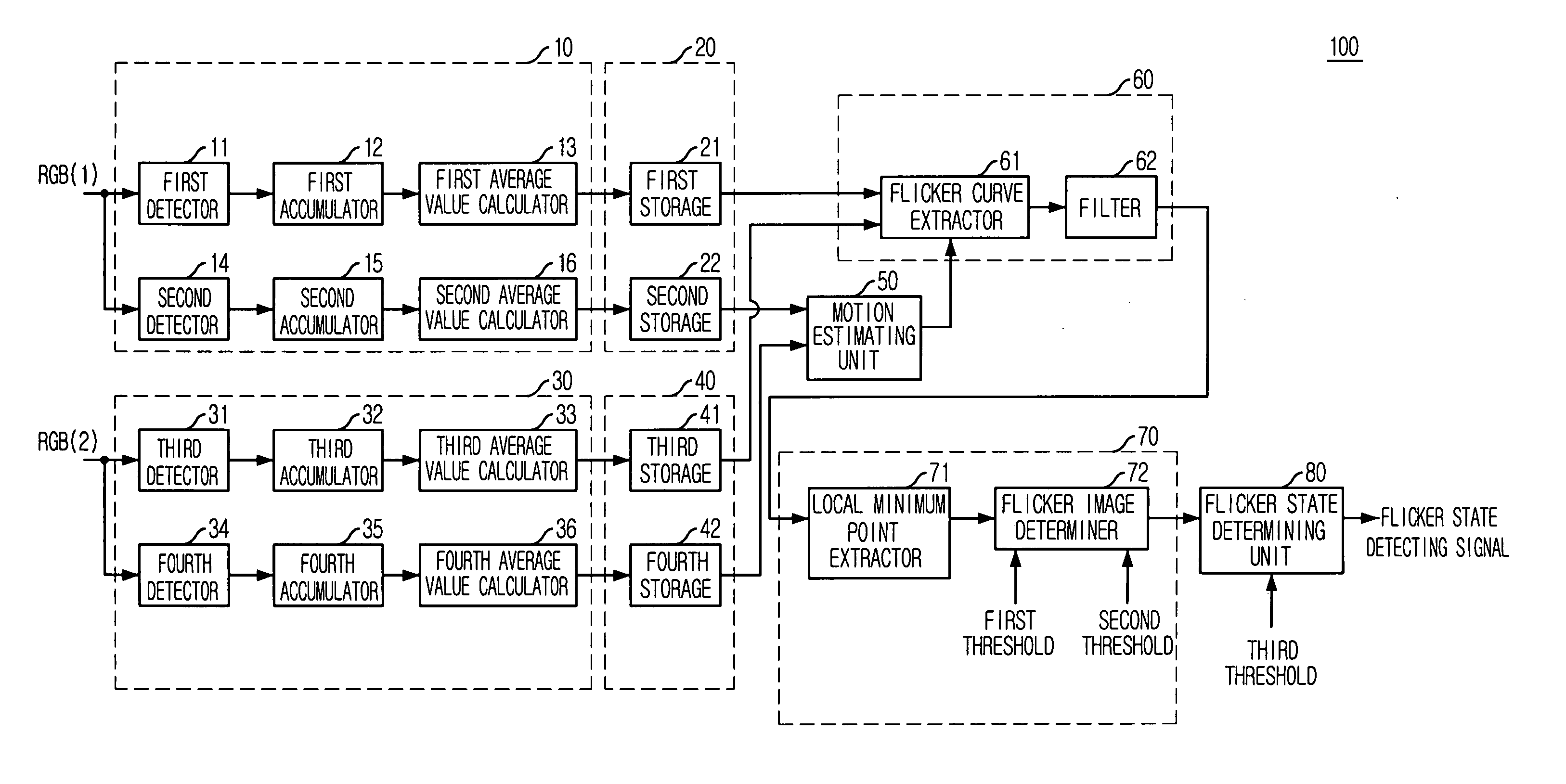
[0038]FIG. 3 is a conceptive view of illustrating a mechanism of detecting a flicker in an image sensor in accordance with a preferred embodiment of the present invention, and FIG. 4 is a block diagram of a flicker detecting circuit in the image sensor in accordance with the preferred embodiment of the present invention.

[0039] In FIG. 3, the mechanism for detecting the flicker in the image senor in accordance with the preferred embodiment of the present invention consecutively photographs one picture several times, e.g., twice, and detects the flicker by subtracting luminance values of a second photographed image (second frame FRAME2) of two photographed images from luminance values of a first photographed image (fir...


PUM


Abstract

A circuit includes a luminance average value output unit for extracting luminance values from pixel data of the first and the second frames to generate first luminance average values for pixel lines of the first frame and second luminance average values for pixel lines of the second frame, a flicker curve generating unit for subtracting the second luminance average values from the first luminance average values, thereby generating a flicker curve, and a flicker detecting unit for extracting a plurality of local minimum points from the flicker curve, calculating a distance between each two neighboring local minimum points of the extracted local minimum points, and determining whether the flicker is present based on the distances and the frequency numbers of the distances.

Description

FIELD OF THE INVENTION [0001] The present invention relates to a semiconductor design technique, and more particularly, a circuit and method for detecting a flicker in a band form in an image sensor. DESCRIPTION OF RELATED ARTS [0002] Recently, a demand of a digital camera has explosively increased with the development of a picture communication using Internet. Moreover, as mobile communications terminals, such as a Personal Digital Assistant (PDA), an International Mobile Telecommunications-2000 (IMT-2000), and a Code Division Multiple Access (CDMA) terminal, in which a camera is built, have been increasingly spread, a demand of a compact camera module has increased. [0003] The camera module essentially includes an image sensor. The image sensor typically is a device for converting an optical image into an electric signal. A Charge Coupled Device (CCD) and a Complementary Metal-Oxide-Semiconductor (CMOS) image sensor are widely used as such an image sensor. [0004] The CCD has disad...

Claims


Application Information

Patent Timeline
Patent Type & Authority Applications(United States)
IPC IPC(8): H04N9/73H04N25/00
CPCH04N5/235H04N5/2357H04N23/745H04N23/70H04N25/60
Inventor LEE, PYEONG-WOOKIM, CHAE-SUNGLEE, JEONG-GUK
Owner INTELLECTUAL VENTURES II
Learn More