[0022] According to a preferred embodiment, the BGR circuit described herein may be configured for reducing any voltage and current offsets that may occur within the BGR circuit as a result of process-induced
transistor mismatch. For example, the
operational amplifier and
current mirror circuits described herein may be implemented primarily with small, low voltage devices to reduce
layout area and enable low power operation. Circuits including such devices are often adversely affected by variations in device characteristics caused, e.g., when variations in process, voltage and / or temperature lead to
transistor mismatch. In some cases, such variations may create large voltage and current offsets within the operational
amplifier and current mirror portions of the Bandgap circuit, thereby reducing the accuracy thereof.
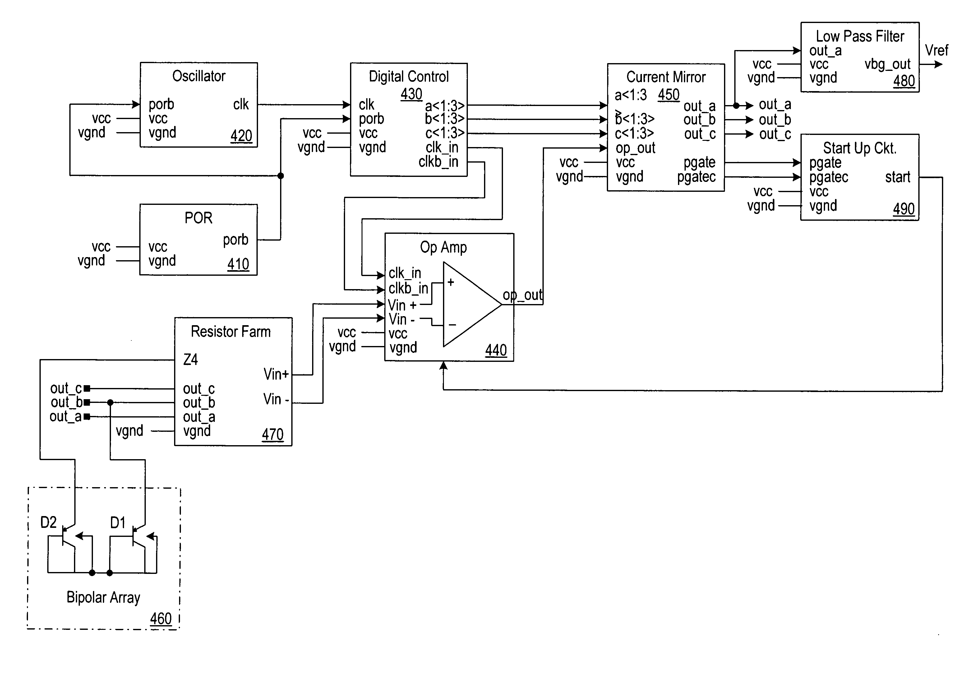
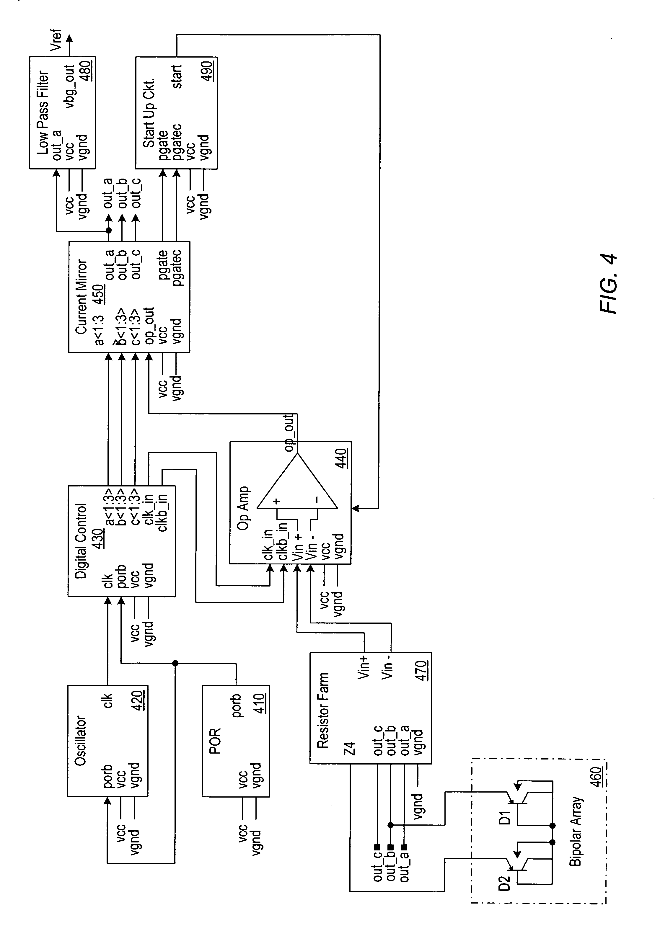
[0023] To improve accuracy, the operational
amplifier (“op amp”) may include a pair of chopped stabilization input circuits for reducing a voltage offset attributed to the small, low voltage devices used within the op amp circuit. In addition, the three-
branch current mirror circuit may include a plurality of dynamically controlled switches for reducing a current offset attributed to the small low voltage devices used within the current mirror circuit. In one embodiment, the plurality of dynamically controlled switches may include three sets of three parallel-coupled switches, where each set of switches is coupled for receiving a different one of the three substantially identical currents.
[0025] In some cases, a first subset of control signals may be supplied to the operational
amplifier for reducing mismatch-
induced voltage offsets by modulating the difference
signal (i.e., the output of the operational amplifier) with a second clocking
signal, whose
duty cycle is about 50% that of the first clocking
signal. In other words, the
digital control block may generate the first subset of control signals by dividing the first clocking signal in half to generate two equal-length phases of the second clocking signal. The first subset of control signals may then be supplied to the pair of chopped stabilization input circuits for reducing any mismatch-
induced voltage offsets that may (or may not) occur within the operational amplifier. For example, the first subset of control signals may be used for generating a positive voltage offset during a first
clock phase and an equally
negative voltage offset during a next
clock phase, where a “
clock phase” is defined herein as one-half of a clock period. In this manner, any voltage offsets occurring within the operational amplifier may be reduced and / or eliminated by averaging the equally positive and
negative voltage offset portions generated over two consecutive phases of the second clocking signal.
[0026] In some cases, the
digital control block may use one of the first subset of control signals to generate a second subset of control signals, corresponding to six distinct phases of a third clocking signal. In other words, the
digital control block may generate the second subset of control signals by dividing one phase of the second clocking signal by six, thereby generating six equal-length phases of the third clocking signal. The second subset of the control signals may then be supplied to the current mirror circuit for reducing any mismatch-induced current offsets that may (or may not) occur within the current mirror circuit. For example, the second subset of control signals may be used for controlling the plurality of switches, such that only one switch within each set of switches is activated for conducting current during each of the six clock phases. In this manner, any current offsets occurring within the current mirror circuit may be reduced and / or eliminated by controlling the activation of switches, so that the three substantially identical currents are averaged over the six consecutive phases of the third clocking signal.
[0027] According to another embodiment, a method is provided herein for reducing mismatch-
induced voltage and current offsets within a current adding Bandgap reference (BGR) circuit comprising a three-
branch current mirror circuit and operational amplifier, as described above. For example, the method may include modulating an output of the operational amplifier with a 50%
duty cycle clocking signal to reduce any voltage offsets attributed to the operational amplifier. In some cases, the method may also include: i) supplying the modulated output of the operational amplifier to the three-
branch current mirror circuit for generating three substantially identical currents in response thereto, and ii) generating a plurality of digital control signals, each representing a different phase of the clocking signal. In a preferred aspect of the invention, the plurality of digital control signals may be used to reduce any current offsets that may (or may not) occur within the current mirror circuit by averaging the three substantially identical currents over all phases of the clocking signal.

