Semiconductor laser device

a laser device and semiconductor technology, applied in semiconductor lasers, laser details, electrical equipment, etc., can solve the problem of poor temperature characteristics of the gainasp semiconductor laser devi

Inactive Publication Date: 2007-07-05
FURUKAWA ELECTRIC CO LTD
View PDF2 Cites 15 Cited by
  • Summary
  • Abstract
  • Description
  • Claims
  • Application Information

AI Technical Summary

Benefits of technology

[0007] It is an object of the present invention to at least partially solve the problems in the conventional technology.

Problems solved by technology

However, the GaInAsP semiconductor laser device has poor temperature characteristics, because a characteristic temperature of the threshold current is in a range of 50K to 70K.

Method used


Image

  • Semiconductor laser device
  • Semiconductor laser device
  • Semiconductor laser device

Examples


first embodiment

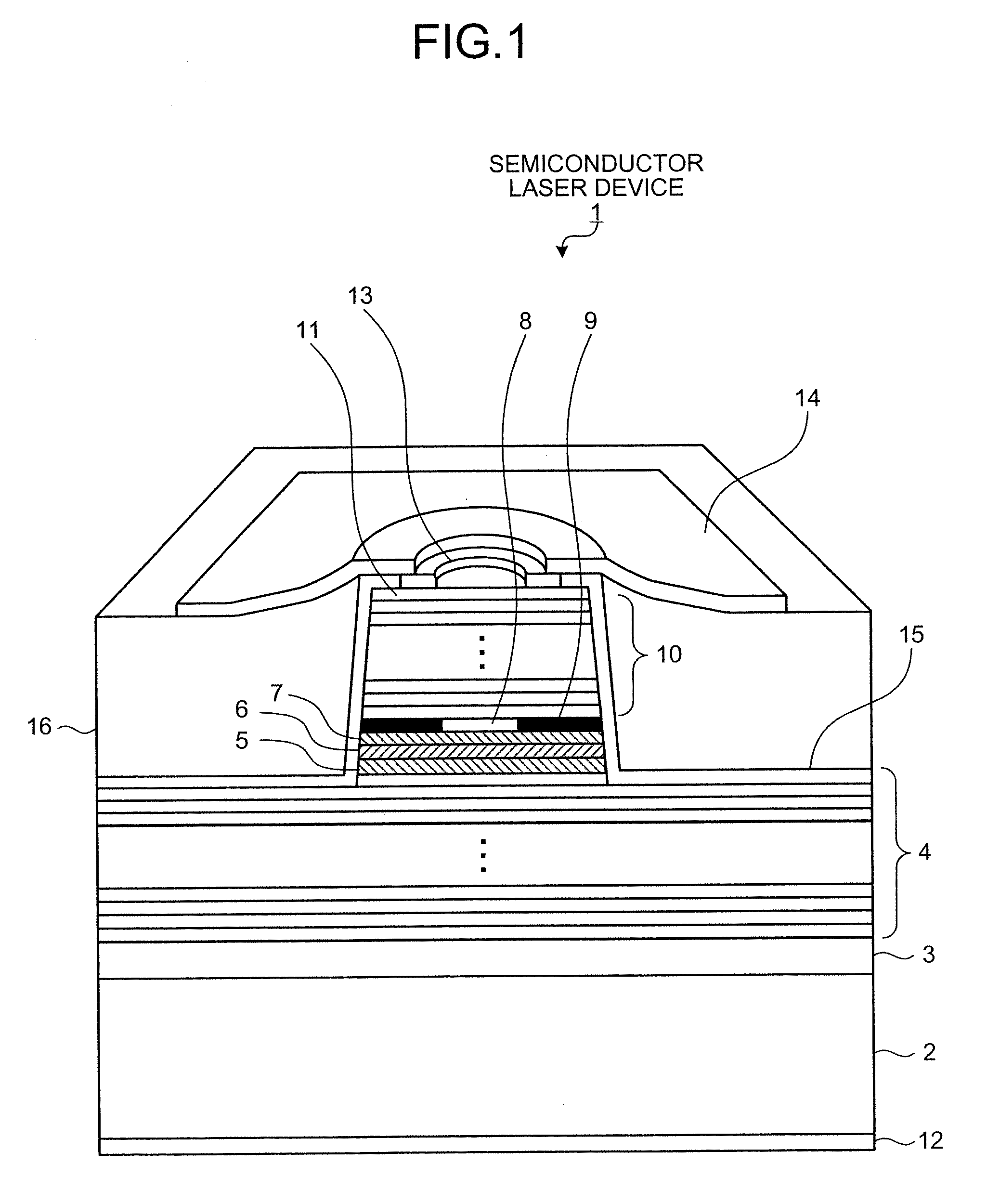
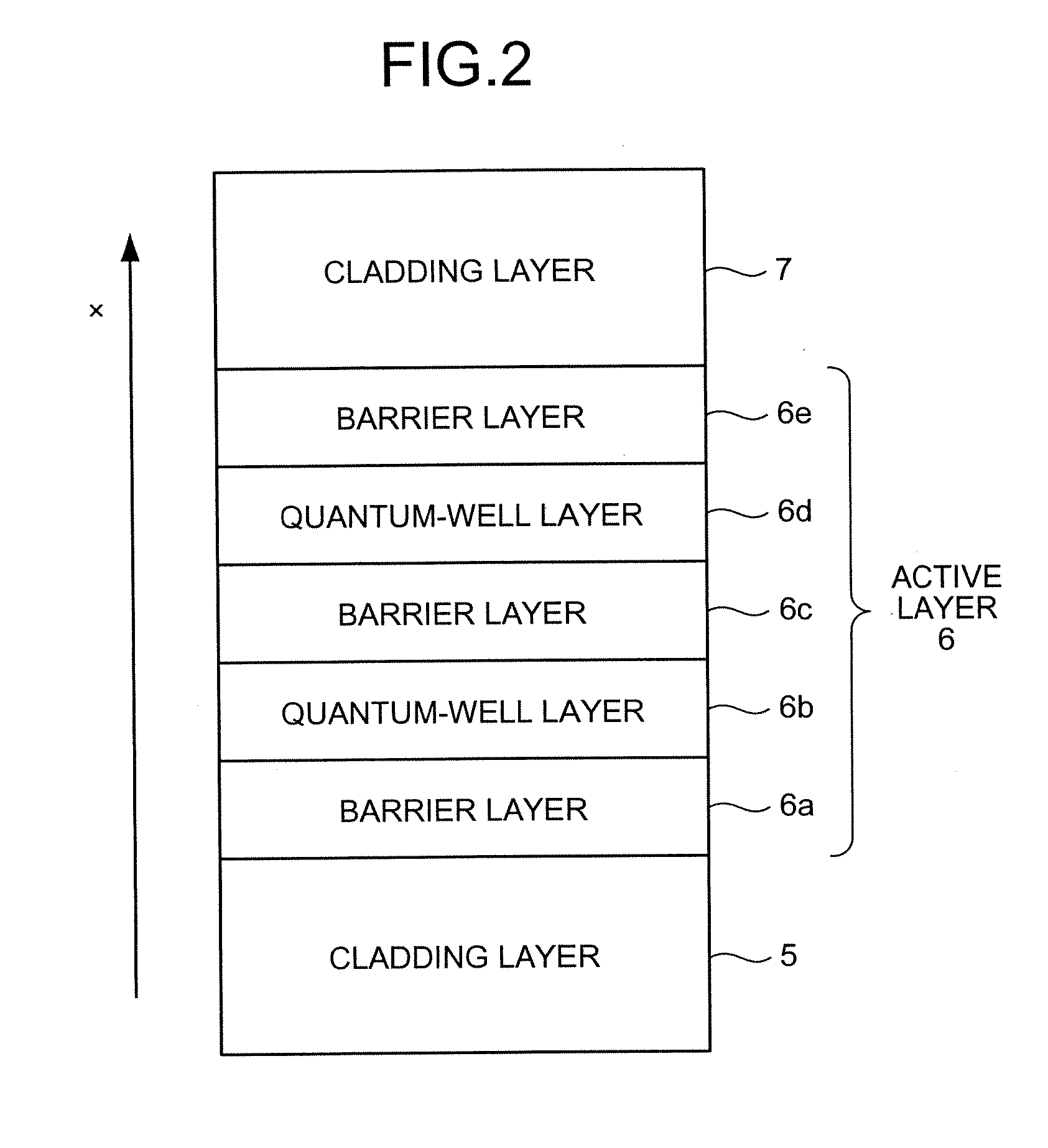
[0024]FIG. 1 is a schematic diagram for explaining a layer structure of a semiconductor laser device 1 according to the present invention. The semiconductor laser device 1 shown in FIG. 1 is a vertical cavity surface emitting laser (VCSEL). FIG. 1 shows an oblique perspective view of a cross section of the semiconductor laser device 1. The semiconductor laser device 1 includes an n-GaAs buffer layer 3, a lower multilayer reflection mirror 4, a cladding layer 5, an active layer 6, a cladding layer 7, a current confinement layer 9 having a current injection path 8, an upper multilayer reflection mirror 10, and a contact layer 11, sequentially grown on an n-GaAs substrate 2. The semiconductor laser device 1 further includes an n-type electrode 12 formed on a bottom of the n-GaAs substrate 2, and a ring-shaped p-type electrode 13 and an electrode pad 14 for drawing the p-type electrode 13 formed on a top of the contact layer 11. A layer area including a top layer of the lower multilayer...

second embodiment

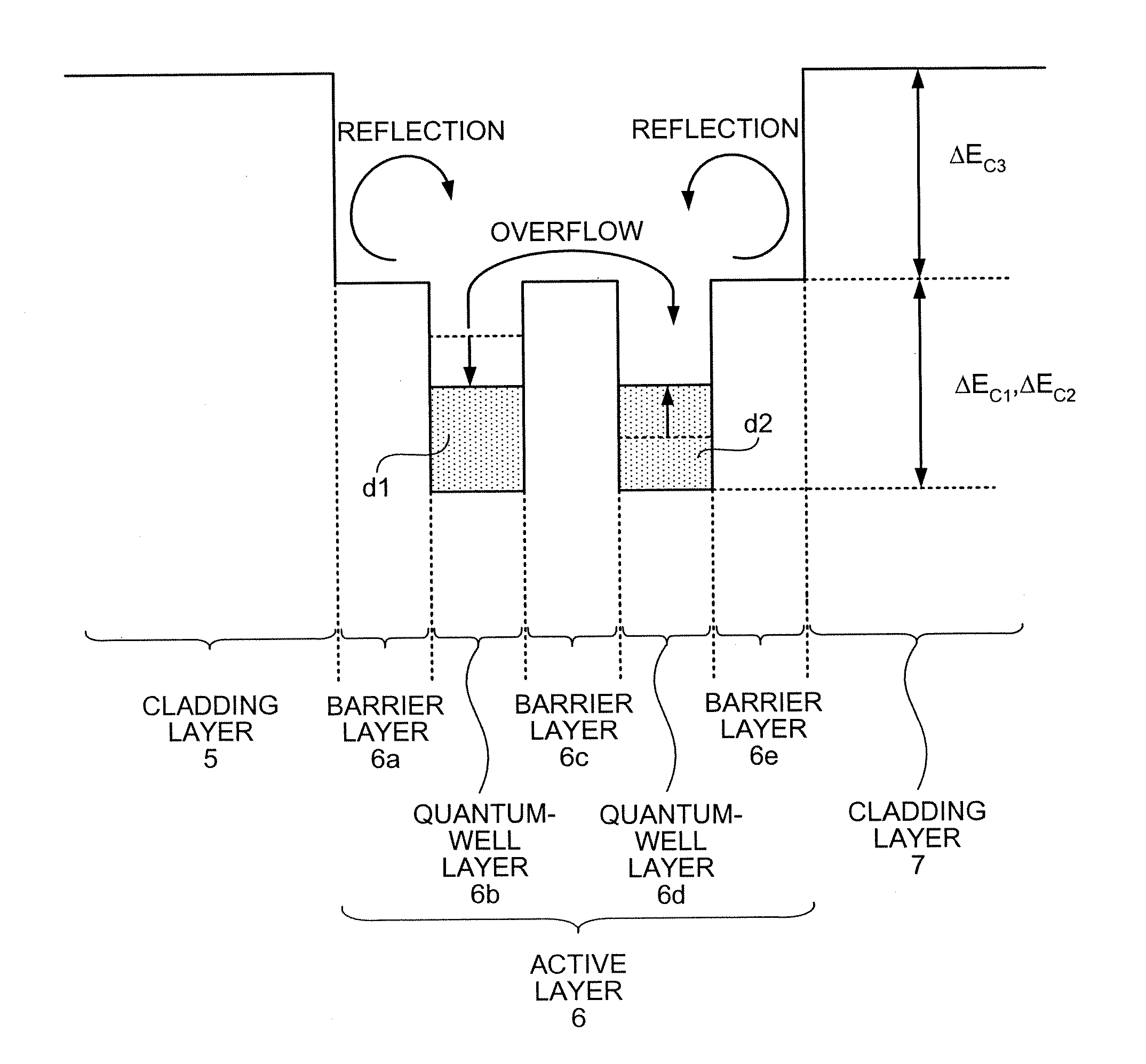
[0092] As shown in FIG. 13, an amount of strain, a layer thickness, and a composition of the layer materials of the barrier layers 66a and 66e are controlled so that the energy level Ec (meV) in the conduction band becomes E4. In this case, the amount of band discontinuity ΔEc2 between the outermost barrier layers 66a and 66e and the quantum-well layers 26b and 26d is set to equal to or more than 300 meV. The barrier layers 66a, and 66e satisfying the condition for the amount of band discontinuity ΔEc2 can bring out the carrier confining function in the quantum-well layers 26b and 26d, in the virtually same way as the case in the second embodiment, and suppress the overflow of the carriers from the quantum-well layers 26b and 26d to the barrier layers 66a and 66e.

[0093] Comparing FIG. 10 and FIG. 13, the profile of the energy level Ec of the semiconductor laser device 61 near the active layer 66, i.e., the energy level profile of the optical-waveguide layers 25 and 27 and the activ...


PUM


Abstract

An active layer is formed by arranging a plurality of quantum-well layers and a plurality of barrier layers alternatively. An amount of band discontinuity in a conduction band between a barrier layer that is sandwiched by the quantum-well layers and adjacent quantum-well layers is equal to or more than 26 meV and less than 300 meV, so that an overflow of injected carriers due to a thermal excitation between the quantum-well layers is intentionally caused to make the carrier density uniform between the quantum-well layers.

Description

BACKGROUND OF THE INVENTION [0001] 1. Field of the Invention [0002] The present invention relates to a technology for reducing a threshold current of a semiconductor laser device that emits a laser light. [0003] 2. Description of the Related Art [0004] A conventional semiconductor laser device emits a laser light by amplifying a light generated by a recombination of carriers in an active layer formed with III-V compound semiconductors with an injection of carriers in the active layer. Generally, because the semiconductor laser device has a number of advantages over a gas laser represented by an excimer laser and a solid-state laser represented by a YAG laser, such as compact size and high electrical-optical conversion efficiency, the semiconductor laser device is currently attracting an attention in a variety of industry fields including the optical communications. [0005] One of the semiconductor laser devices used as a light source for an optical communication device emits a laser ...

Claims


Application Information

Patent Timeline
Patent Type & Authority Applications(United States)
IPC IPC(8): H01S5/00
CPCB82Y20/00H01S5/18311H01S5/2004H01S5/34306H01S5/22H01S5/3211H01S5/3415H01S5/2009
Inventor KAGEYAMA, TAKEOIKENAGA, YOSHIHIKO
Owner FURUKAWA ELECTRIC CO LTD
Why Eureka
Try Eureka