Patterning method and method for manufacturing liquid crystal display device using the same

a technology of liquid crystal display and patterning method, which is applied in the direction of originals for photomechanical treatment, instruments, lithography, etc., can solve the problems of increasing the manufacturing cost of an lcd device, photolithography requires exposure, and increasing the manufacturing time of lcd devices, so as to reduce the cost and waste of materials, improve the accuracy of printing

Active Publication Date: 2007-07-12
LG DISPLAY CO LTD
View PDF15 Cites 9 Cited by
  • Summary
  • Abstract
  • Description
  • Claims
  • Application Information

AI Technical Summary

Benefits of technology

[0027] An advantage of the present invention is to provide a patterning method and a method for manufacturing an LCD device using the same, to improve the preciseness of printing, and to reduce cost and waste of material.
[0028] Additional features and advantages of the invention will be set forth in the description which follows, and in part will be apparent from the description, or may be learned by practice of the invention. The objectives and other advantages of the invention will be realized and attained by the structure particularly pointed out in the written description and claims hereof as well as the appended drawings.
[0029] To achieve these and other advantages and in accordance with the purpose of the present invention, as embodied and broadly described, a patterning method includes: preparing a printing plate having recesses and lands; dropping a pattern material in the recesses of the printing plate; rolling a printing roller on the printing plate to print the pattern material in the recesses onto the printing roller; and rolling the printing roller on a substrate to print the pattern material on the printing roller onto the substrate.
[0030] In another aspect of the presen...

Problems solved by technology

The above photolithographic process uses a photoresist layer and a mask with the predetermined pattern that increases the manufacturing cost for an LCD device.
In addition, photolithography requires exposure and development, which are complicated processes that increase the manufacturing time of LCD devices.
The removal of pattern material 20b from the surface of the pr...

Method used


Image

  • Patterning method and method for manufacturing liquid crystal display device using the same
  • Patterning method and method for manufacturing liquid crystal display device using the same
  • Patterning method and method for manufacturing liquid crystal display device using the same

Examples


first embodiment

[0040]FIGS. 3A to 3D are cross sectional views illustrating a patterning method according to the present invention.

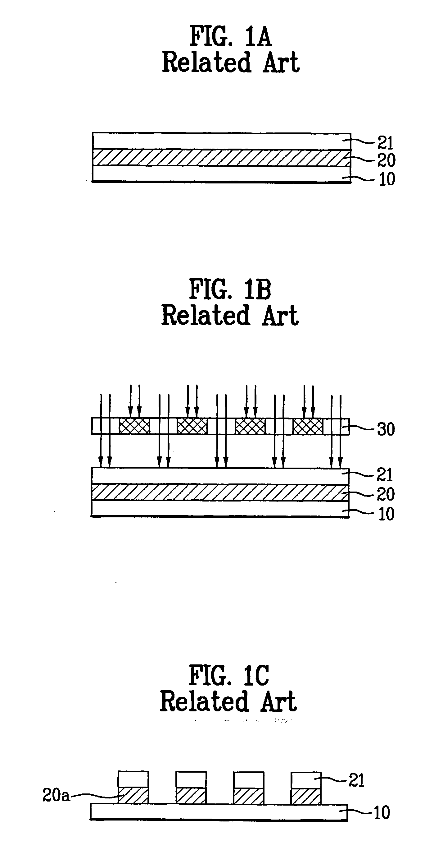
[0041] In the patterning method according to the first embodiment of the present invention, a predetermined material layer is formed on a predetermined portion of a substrate excluding a pattern area, and a hydrophobic material is coated on a surface of the predetermined material layer. A pattern material layer is formed on the substrate excluding the predetermined material layer using an ink-jet method, whereby the pattern material layer is printed on a printing roller. For example, the predetermined material layer may be formed of a black matrix layer.

[0042] As shown in FIG. 3A, the black matrix layer 230 is formed on a hydrophilic substrate 100 excluding the pattern area. The black matrix layer 230 may be formed using photolithography.

[0043] As shown in FIG. 3B, a hydrophobic treatment is applied to the surface of the black matrix layer 230, to thereby form a hydro...

second embodiment

[0050]FIGS. 4A to 4D are cross sectional views of illustrating a patterning method according to the present invention.

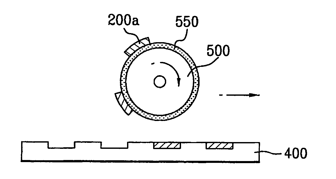
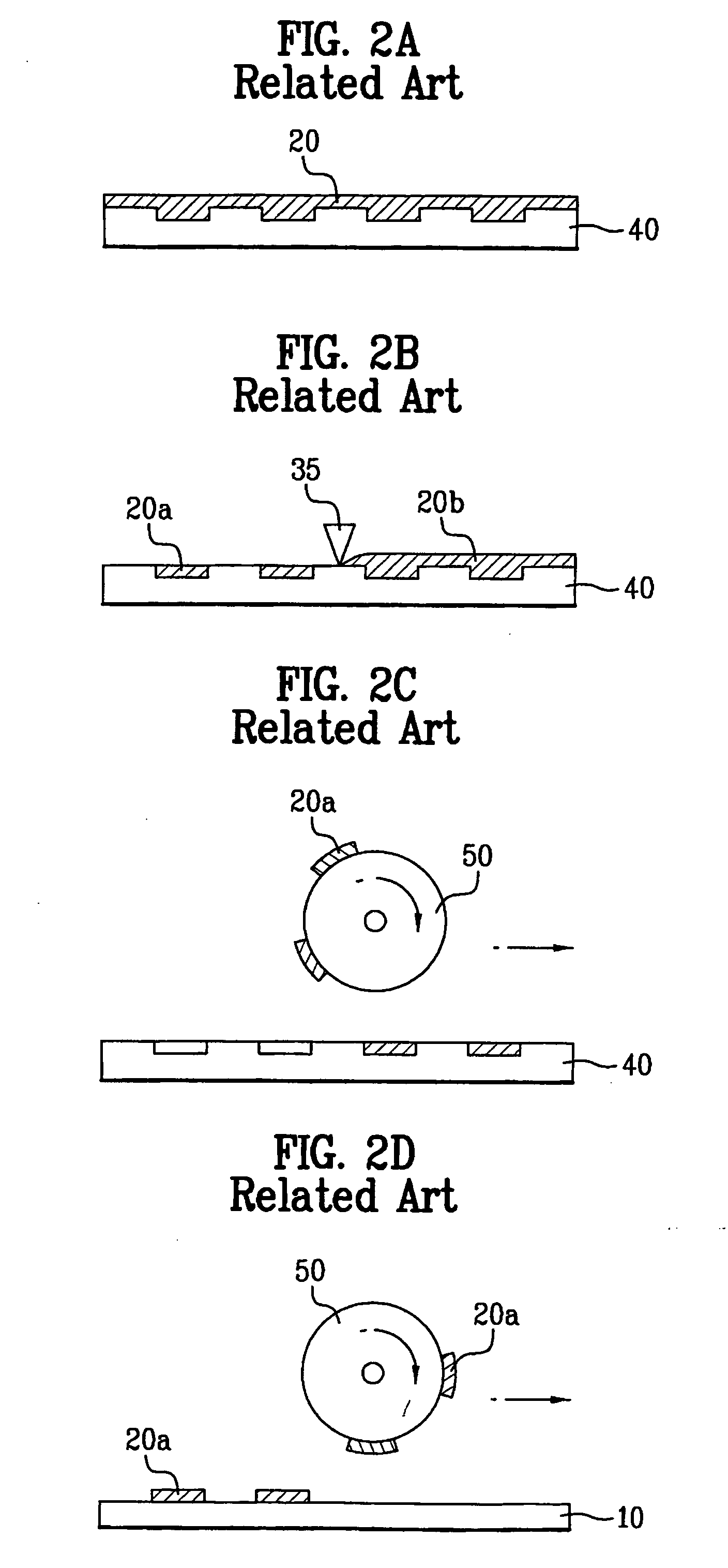
[0051] As shown in FIG. 4A, a printing plate 400 having recesses 430 and lands 460 is prepared. The printing plate 400 may be formed from a glass, organic or inorganic material.

[0052] The bottom of a recess 430 formed in the printing plate 400 may be hydrophilic. By forming printing plate 400 of material having a strong hydrophilic property, performing an additional hydrophilic treatment to the bottom of the recess 430 of the printing plate 400 may be avoided. However, if the printing plate 400 is formed of a hydroxyl-based or carbonyl-based organic material, a hydrophilic treatment using oxygen plasma may be applied to the bottom of a recess 430 of the printing plate 400.

[0053] When the bottom of the recesses 430 of the printing plate 400 have a strong hydrophilic property, the pattern material effectively spreads over the bottom of the recesses 430.

[0054] The pr...


PUM

PropertyMeasurementUnit
Heightaaaaaaaaaa
Hydrophilicityaaaaaaaaaa
Hydrophobicityaaaaaaaaaa

Abstract

A patterning method and a method for manufacturing an LCD device using the same are disclosed. The patterning method includes preparing a printing plate having concave and convex portions; coating a pattern material in the concave portion of the printing plate; rolling a printing roller on the printing plate to print the pattern material of the concave portion on the printing roller; and rolling the printing roller on a substrate to print the pattern material of the printing roller on the substrate.

Description

[0001] This application claims the benefit of Korean Patent Application No. P2005-134118, filed on Dec. 29, 2005, which is hereby incorporated by reference for all purposes as if fully set forth herein. BACKGROUND OF THE INVENTION [0002] 1. Field of the Invention [0003] The present invention relates to liquid crystal display (LCD) devices, and more particularly, to a patterning method for an LCD device. [0004] 2. Discussion of the Related Art [0005] Among various ultra-thin flat type display devices, which include a display screen having a thickness of no more than several centimeters, liquid crystal display (LCD) devices are widely used for notebook computers, monitors, aircraft, etc. because they have advantages such as low power consumption and portability. [0006] An LCD device includes lower and upper substrates facing each other at a predetermined interval therebetween, and a liquid crystal layer formed between the lower and upper substrates. [0007] The lower substrate includes...

Claims


Application Information

Patent Timeline
IPC IPC(8): B41F3/34B41F3/20B41F17/14B41M1/10B41M1/34B41N1/12G02B5/20G02F1/1335G03F1/92H05K3/12H05K3/20
CPCG02B5/201B41M5/0256G02F1/133512G02F1/133516H05K3/125H05K3/1275H05K3/207H05K2203/0113H05K2203/013H05K2203/0143H05K2203/0534H05K2203/1173B41F3/36B41M1/02B41M1/04B41M3/003G02B5/223B41F17/00B41F31/08B41M1/10B41M1/26B41M1/34G02F1/13G02F1/1333G02F1/136
Inventor YOO, HONG SUKKIM, CHUL HOLEE, JUNG JAEOH, TAE YOUNGPARK, CHOON HO
Owner LG DISPLAY CO LTD
Why Eureka
Try Eureka