Image sensor with improved surface depletion

a surface depletion and image sensor technology, applied in the field of imager devices, can solve the problems of difficult to create the pinning effect in the photodiode, cross-talk between pixels, and complex optimization problems of the photodiode and the transfer gate region, and achieve the effect of facilitating the pinning

Active Publication Date: 2007-07-12
APTINA IMAGING CORP
View PDF14 Cites 31 Cited by
  • Summary
  • Abstract
  • Description
  • Claims
  • Application Information

AI Technical Summary

Problems solved by technology

This presents two issues: compensation of n- diode region, and therefore, reduced fill factor; and deeper p+ / n junction, which leads to complex optimization issues for the photodiode and transfer gate region.
As image sensors having pinned photodiodes are scaled down, the photodiode necessarily gets a smaller and it becomes harder to create the pinning effect in the photodiode as the charge accumulating n-type region of the photodiode nears the surface of the substrate.
However, such changes in photodiode shape can lead to cross-talk between pixels as the photodiodes expand below the isolation structures (e.g., shallow trench isolation—STI).

Method used


Image

  • Image sensor with improved surface depletion
  • Image sensor with improved surface depletion
  • Image sensor with improved surface depletion

Examples


Embodiment Construction

[0016] Although this invention will be described in terms of certain exemplary embodiments, other embodiments will be apparent to those of ordinary skill in the art, which also are within the scope of this invention. Accordingly, the scope of the invention is defined only by reference to the appended claims.

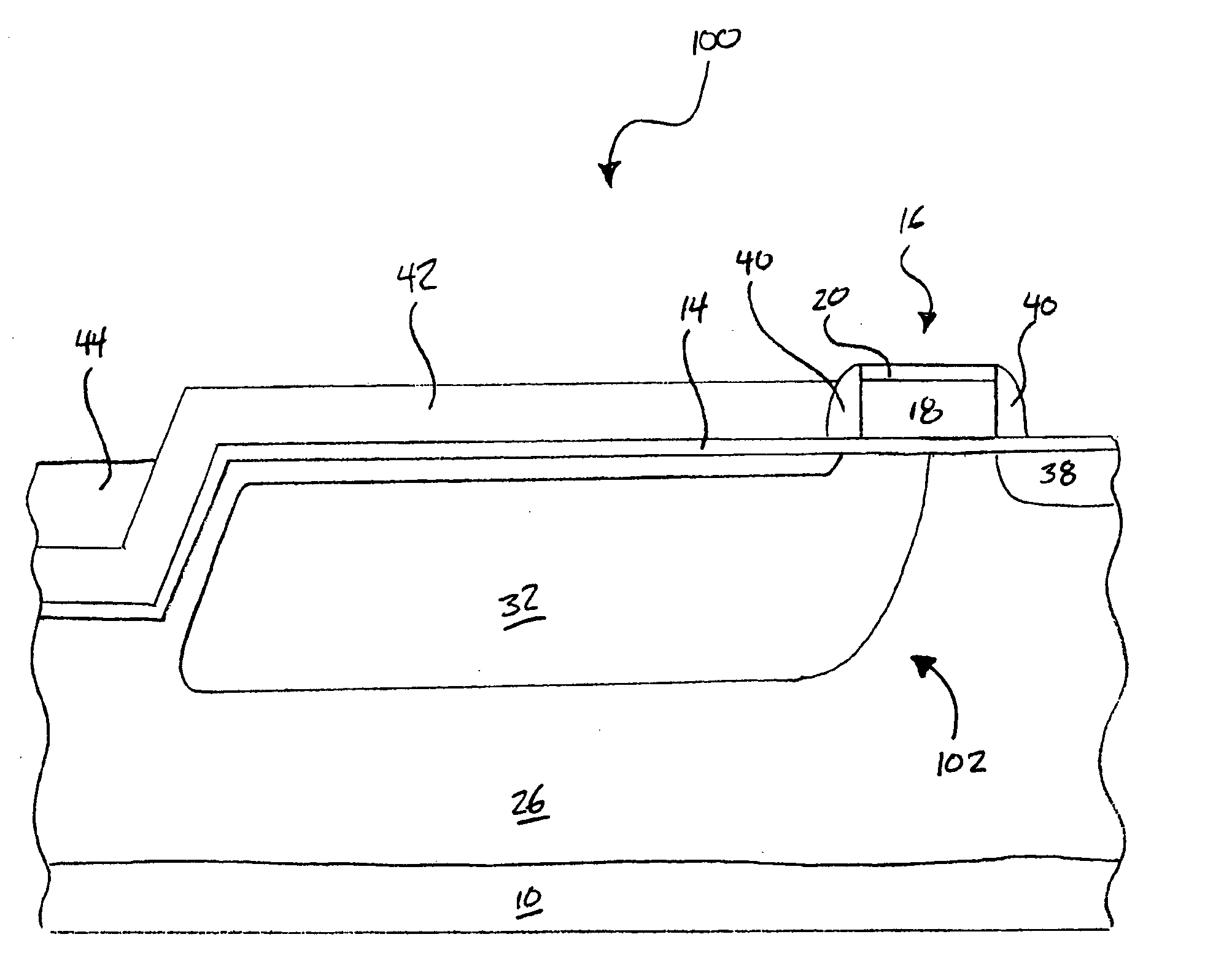
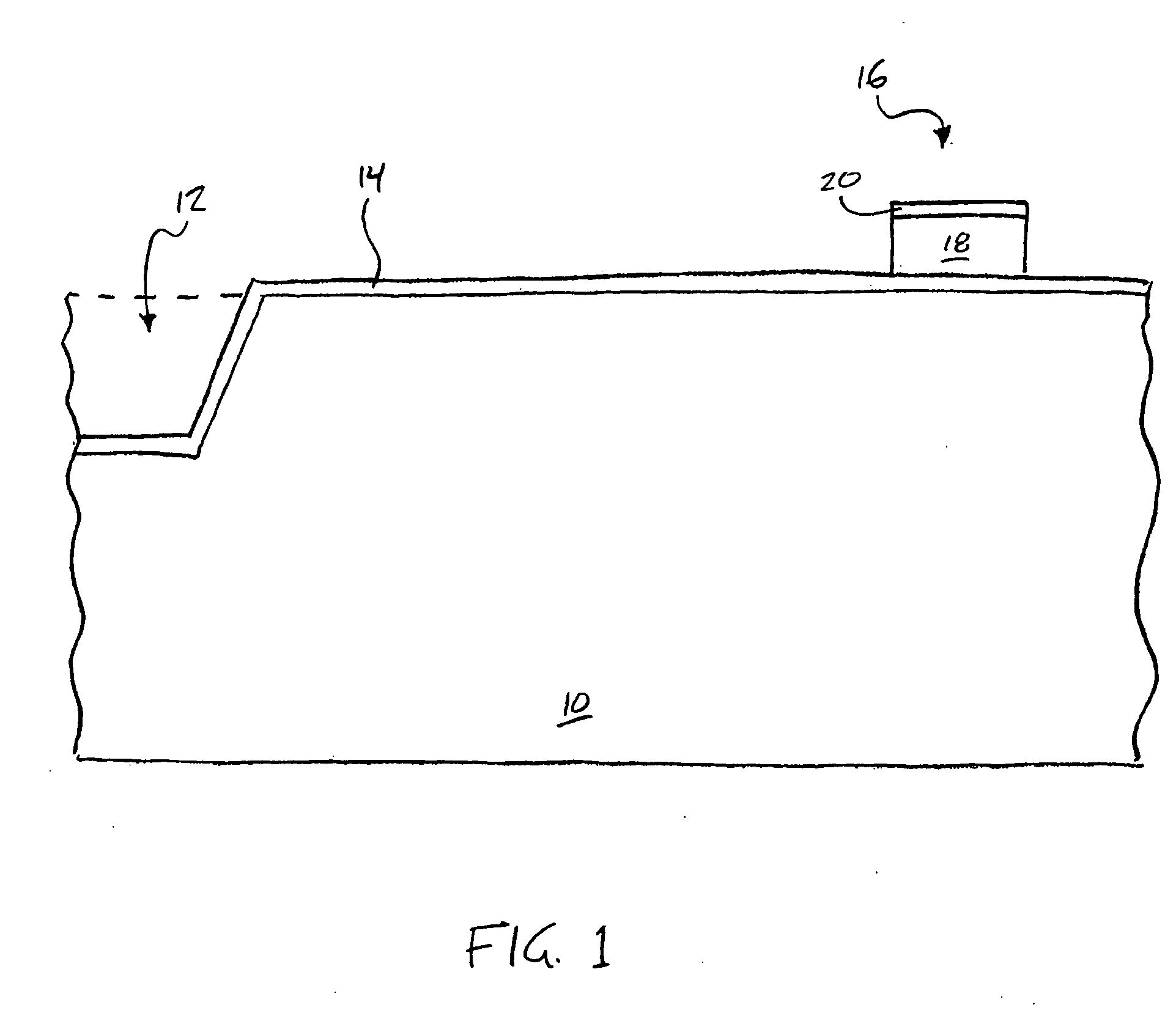
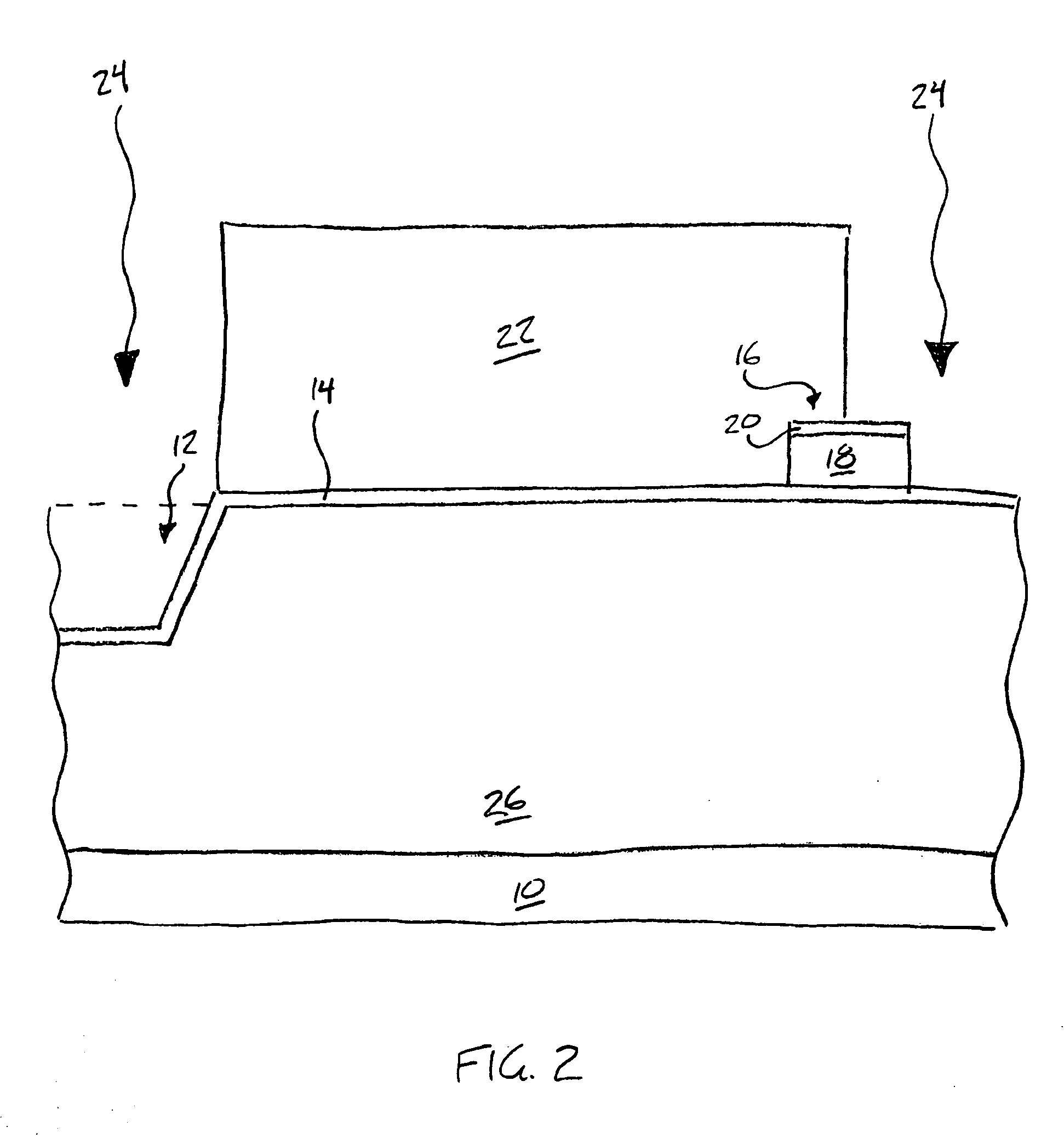
[0017] The term “substrate” in the following description refers to any supporting layer suitable for fabricating an integrated circuit, typically semiconductor based, but not necessarily so. A substrate may be silicon-based, may include epitaxial layers of silicon supported by a base semiconductor foundation, can be sapphire-based, silicon-on-insulator (SOI), metal, polymer, or any other materials suitable for supporting an integrated circuit or image sensor. When reference is made to a substrate or wafer in the following description, previous process steps may have been utilized to form regions or junctions in or over a base semiconductor or foundation.

[0018] The term “pixel” ...


PUM


Abstract

An image sensor device having a pixel cell with a pinned photodiode, which utilizes the fixed charge of an high K dielectric layer over the n-type region for the pinning effect without implanting a p-type layer over the n-type region, and methods of forming such a device.

Description

FIELD OF THE INVENTION [0001] The invention relates to imager technology. In particular, the invention relates to imager devices with a pinned photodiode. BACKGROUND OF THE INVENTION [0002] CMOS imagers are known in the art. Exemplary CMOS imaging circuits, processing steps thereof, and detailed descriptions of the functions of various CMOS elements of an imaging circuit are described, for example, in U.S. Pat. No. 6,140,630, U.S. Pat. No. 6,376,868, U.S. Pat. No. 6,310,366, U.S. Pat. No. 6,326,652, U.S. Pat. No. 6,204,524, and U.S. Pat. No. 6,333,205, each assigned to Micron Technology, Inc. The disclosures of the forgoing patents are hereby incorporated by reference in their entirety. [0003] A typical pixel of a CMOS image sensor cell, in a 4T (four transistor) layout, includes a photodiode as a photoconversion device, a transfer gate for transferring photoelectric charges generated in the charge accumulating region of the photodiode to a floating diffusion region (sensing node). ...

Claims


Application Information

Patent Timeline
Patent Type & Authority Applications(United States)
IPC IPC(8): H01L31/113H01L21/00
CPCH01L27/14601H01L27/14643H01L27/1462H01L27/14609H01L27/146
Inventor MOULI, CHANDRA
Owner APTINA IMAGING CORP
Why Eureka
Try Eureka