Semiconductor device and manufacturing method thereof

a technology of semiconductor devices and semiconductors, applied in semiconductor devices, electrical devices, transistors, etc., can solve the problems of complex gate material selection, inability to relatively increase the impurity concentration of the channel region, and the full-depletion type of soi devices

Inactive Publication Date: 2005-12-08
SHIMAMOTO SATOSHI +1
View PDF2 Cites 26 Cited by
  • Summary
  • Abstract
  • Description
  • Claims
  • Application Information

AI Technical Summary

Benefits of technology

[0006] In the full-depletion type SOI device, since the SOI layer is depleted, an impurity concentration in the channel region cannot be relatively increased and a threshold voltage is determined based on the impurity concentration in the channel region formed in the SOI layer with a thickness of 50 nm or less. Therefore, only the MISFET having the threshold voltage on a significantly depletion side can be obtained. However, in consideration of reductions of a LSI (Large Sc...

Problems solved by technology

However, the full-depletion type SOI device has various technical problems as described below.
However, the impurity concentration of the channel region cannot be relatively increased in order to keep the SOI layer in a full depletion state or to use a characteristic such as a small substrate effect constant.
However, in order to form a plurality of MISFETs with mutually different threshold voltages, i...

Method used


Image

  • Semiconductor device and manufacturing method thereof
  • Semiconductor device and manufacturing method thereof
  • Semiconductor device and manufacturing method thereof

Examples


first embodiment

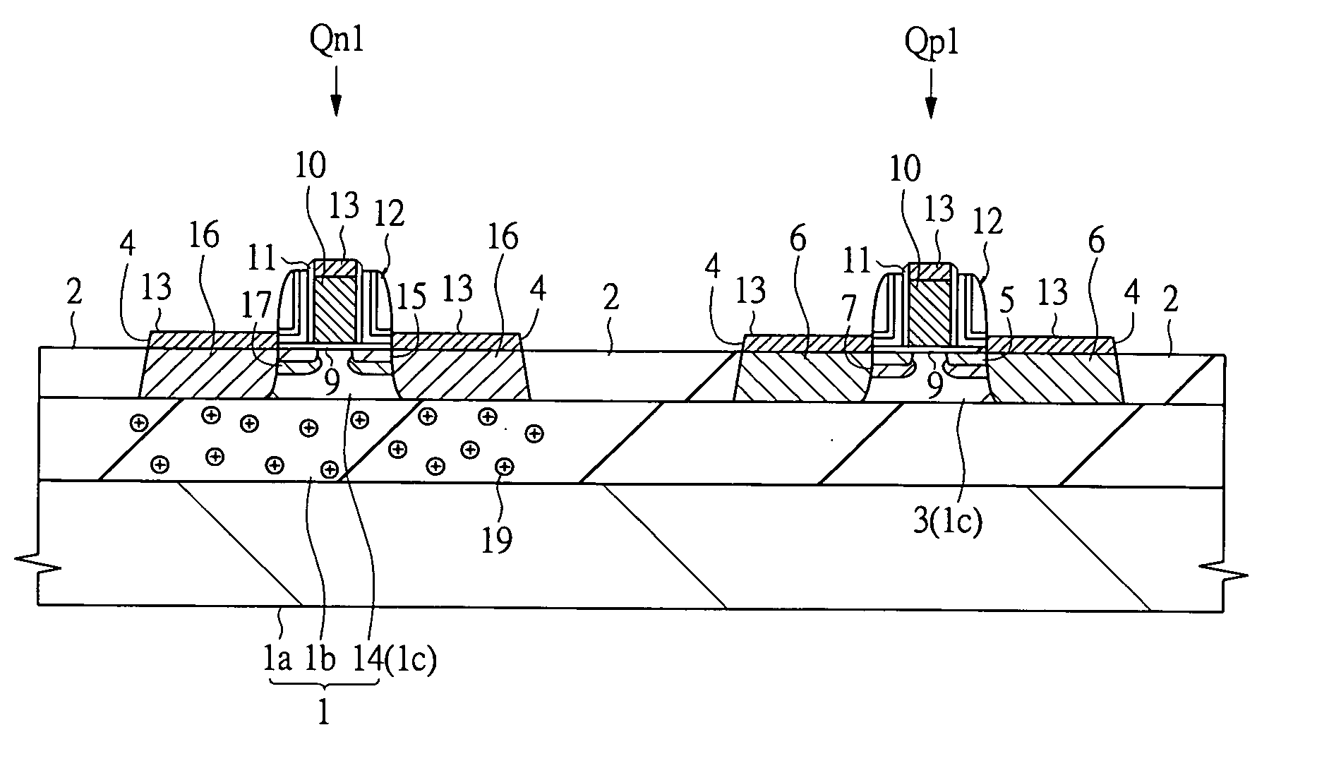
[0062]FIG. 1 is a sectional view of a principal portion of a SOI substrate showing a full-depletion type SOI device according to a first embodiment. A CMOS device is illustrated as the full-depletion type SOI device and the reference symbol “Qp1” is a pMIS and “Qn1” is an nMIS in FIG. 1.

[0063] The pMIS Qp1 and nMIS Qn1 are formed on a SOI substrate 1 manufactured by, for example, a SIMOX (Separation by Implanted Oxygen) method. The SOI substrate 1 is constituted so that a SOI layer (or body layer) 1c is formed on a supporting substrate la through a BOX (Buried Oxide) layer 1b. The BOX layer 1b is made of an insulating material having a thickness of, for example, approximately 100 nm and the SOI layer 1c is made of single crystal silicon having a thickness of, for example, 50 nm or less.

[0064] The pMIS Qp1 is formed on the SOI layer 1c and is formed in an n-type well 3 surrounded by device isolation 2. A silicon layer 4 is stacked on the n-type well 3 by a selective epitaxial growt...

second embodiment

[0090] In the above-described first embodiment, the material having a work function approximate to that of the channel region of the pMIS Qp1, such as molybdenum or ruthenium, is used as a gate material of each gate electrode 10 of the pMIS Qp1 and nMIS Qn1 to control the threshold voltage of the pMIS Qp1, and the threshold voltage of the nMIS Qn1 is controlled by the positive fixed charges 19 induced in the BOX layer 1b under the p-type well 14. However, in this second embodiment, a material having a work function approximate to that of the channel region of the nMIS, such as platinum (Pt) or lead (Pb), is used as a gate material of each of the PMIS and nMIS to control the threshold voltage of the nMIS, and the threshold voltage of the pMIS is controlled by negative fixed charges induced in the BOX layer.

[0091] The second embodiment will be described with reference to FIG. 16. FIG. 16 is a sectional view of a principal portion of a SOI substrate showing a full-depletion type SOI d...

third embodiment

[0094]FIG. 18 is a sectional view of a principal portion of a SOI substrate showing a full-depletion type SOI device according to a third embodiment. A CMOS device is illustrated as the full-depletion type SOI device. A pMIS Qp3 and an nMIS Qn3 have relatively high threshold voltages and a pMIS Qp4 and an nMIS Qn4 have relatively low threshold voltages. Note that the third embodiment, excluding the constitution of the gate electrode and the fixed charges induced in the BOX layer, is identical to the first embodiment and therefore the explanation thereof will be omitted.

[0095] Two pMISs Qp3 and Qp4 and two nMISs Qn3 and Qn4 are formed on the SOI substrate 1. Materials having work functions approximate to those of channel regions of the pMISs Qp3 and Qp4, such as molybdenum or ruthenium, are used as gate materials of gate electrodes 27p of the pMISs Qp3 and Qp4. Since positive fixed charges are induced in the BOX layer 1b under an n-type well 28 in which the pMIS Qp3 is formed, the p...


PUM


Abstract

A technique for forming a plurality of MISFETs having desired threshold voltages on a SOI substrate is provided. Each gate electrodes of pMIS and nMIS is made of a metal film having a work function approximate to that of a channel region of the pMIS, such as a molybdenum or ruthenium film, and a rise of the threshold voltage due to the metal film is reduced by inducing a positive fixed charge in a BOX layer. Thereby, the pMIS and nMIS having the desired threshold voltages can be formed on the SOI substrate.

Description

CROSS-REFERENCE TO RELATED APPLICATION [0001] The present application claims priority from Japanese patent application No. JP 2004-166879 filed on Jun. 4, 2004, the content of which is hereby incorporated by reference into this application. BACKGROUND OF THE INVENTION [0002] The present invention relates to a semiconductor device and a manufacturing method thereof and especially to a technique effectively applied to manufacture of a MISFET (Metal Insulator Semiconductor Field Effect Transistor) formed on a SOI (Silicon On Insulator) substrate. [0003] When a CMOS (Complementary Metal Oxide Semiconductor) device with a gate length of 65 nm or less conforms to a conventional scaling law, device performance is difficult to improve and there arises a problem that the device performance is deteriorated to the contrary. In the CMOS device with a gate length of, for example, 40 nm, a halo region with a relatively high concentration is formed on each bottom of source and drain regions in ord...

Claims


Application Information

Patent Timeline
IPC IPC(8): H01L21/8238H01L27/08H01L21/84H01L27/01H01L27/092H01L27/12H01L29/786
CPCH01L27/1203H01L21/84
Inventor SHIMAMOTO, SATOSHIICHINOSE, KATSUHIKO
Owner SHIMAMOTO SATOSHI
Why Eureka
Try Eureka