Thin film transistor, electronic device having the same, and method for manufacturing the same

a technology of thin film transistors and electronic devices, applied in the direction of semiconductor devices, basic electric elements, electrical equipment, etc., can solve the problems of gate leakage current, misalignment, and film fine enough to be generally used as gate insulating films, etc., to reduce fixed charges, reduce interface levels, and reduce gate leakage current

Inactive Publication Date: 2005-01-20
SEMICON ENERGY LAB CO LTD
View PDF16 Cites 25 Cited by
  • Summary
  • Abstract
  • Description
  • Claims
  • Application Information

AI Technical Summary

Benefits of technology

[0029] According to the present invention having the above structures, a gate insulating film can be heat-treated without a problem of an alignment defect in patterning even at a temperature of 700° C. that conventionally causes a problem of misalignment in patterning due to shrinkage of a substrate such as glass.
[0030] In the present invention, a gate insulating film can be heat-treated at a temperature of 700° C. above a strain point of a substrate such as glass. Therefore, an interface level is lowered; a fixed charge is reduced; a gate leakage current is lowered; field-effect mobility, subthreshold coefficient, and the like become favorable; a change of transistor characteristics over time during continuous operation can be reduced; a yield is improved; and variation in the characteristics is reduced, in a thin film transistor.

Problems solved by technology

This is because a processing temperature is restricted in terms of heat resistance of glass or the like that is a substrate over which an integrated circuit is formed as well as because of a crystallinity problem of a silicon film (polycrystalline silicon film or the like) for manufacturing an integrated circuit.
A gate insulating film which is fine and has good electrical adequacy can be formed by a CVD method, but a film formation temperature is required to be equal to or more than 750° C. A plasma CVD method makes it possible to form a film at a low temperature; however, it is a problem that a film is damaged by a charged particle in plasma and a defect or a pinhole is easily caused.
However, a film fine enough to be generally used as a gate insulating film is not obtained by a radio frequency sputtering method in comparison with a CVD method.
However, a substrate such as glass that expands or shrinks before or after applying a temperature above a strain point has a problem that misalignment occurs in patterning a film formed over the substrate.
Therefore, it is difficult to heat-treat a gate insulating film at a temperature above a strain point of the substrate.

Method used


Image

  • Thin film transistor, electronic device having the same, and method for manufacturing the same
  • Thin film transistor, electronic device having the same, and method for manufacturing the same
  • Thin film transistor, electronic device having the same, and method for manufacturing the same

Examples


embodiment

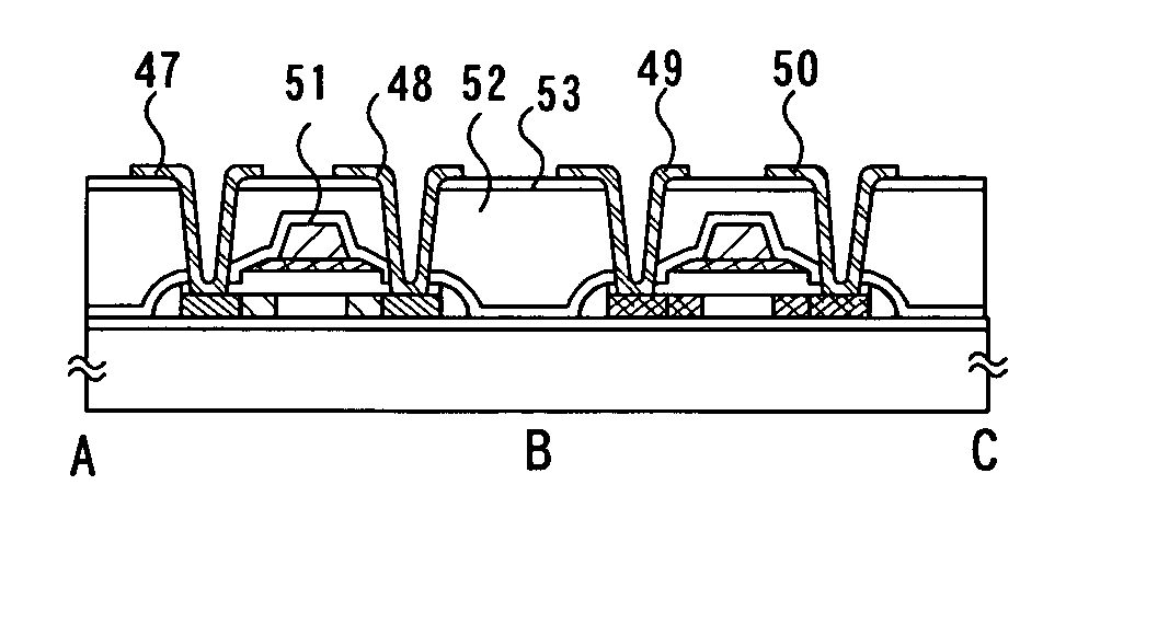
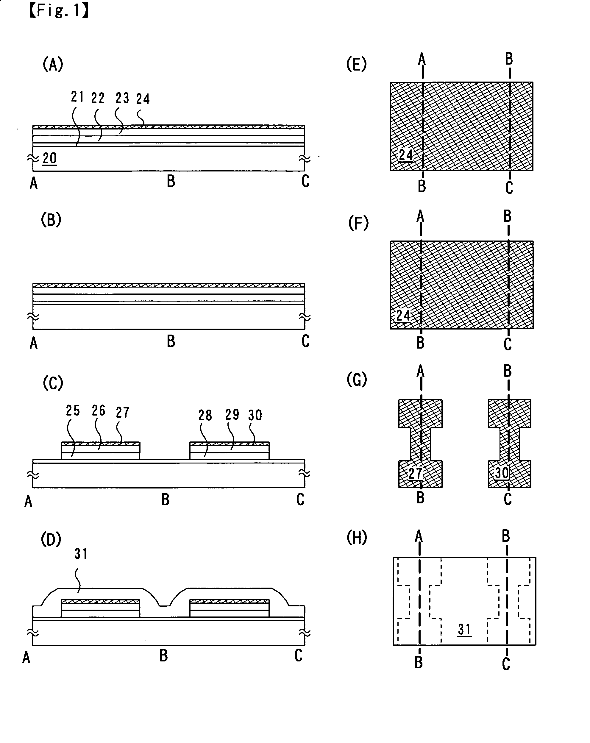
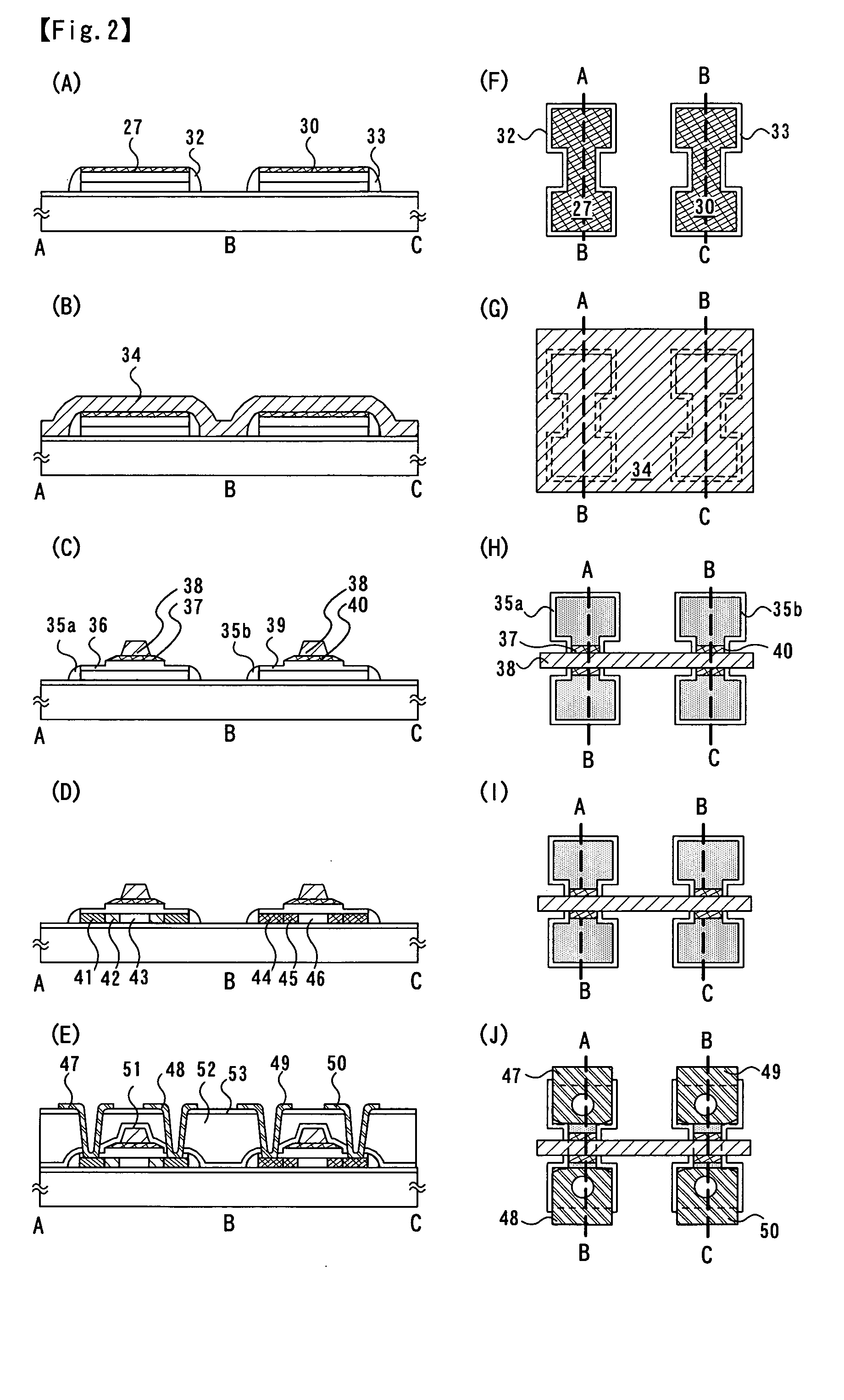
[0038] Embodiment Mode 1

[0039] A glass substrate made of a material such as barium borosilicate glass, alumino borosilicate glass, or aluminosilicate glass, or the like can be given as a substrate which can be applied in this embodiment mode. Typically, a 1737 glass substrate (strain point: 667° C.) manufactured by Corning, Inc., AN100 (strain point: 670° C.) manufactured by Asahi Glass Co., Ltd., or the like can be applied, but there is no particular limitation on other similar substrates.

[0040] A first inorganic insulating layer 21 made of an insulating film such as a silicon oxide film, a silicon nitride film, or a silicon oxynitride film (SiOxNy) is formed over a glass substrate 20, as shown in FIGS. 1(A) and 1(E), using the above substrate. A typical example of the first inorganic insulating layer 21 has a two-layer structure, which is a structure where a first silicon oxynitride film formed to be 50 nm in thickness by a plasma CVD method using SiH4, NH3, and N2O as a reactive...

embodiment 2

[0072] Embodiment 2

[0073] An embodiment of the present invention is described with reference to FIG. 5. FIG. 5(A) is a top view of a display panel formed by sealing a substrate over which a TFT is formed with a sealing material. FIG. 5(B) is a cross-sectional view along a line B-B′ in FIG. 5(A). FIGS. 5(C) and 5(D) are cross-sectional views along a line A-A′ in FIG. 5(A). Note that FIG. 5(C) is a cross-sectional view of a display panel performing bottom emission in which light is emitted in a direction of the substrate over which a TFT is formed. FIG. 5(D) is a cross-sectional view of a display panel performing top emission in which light is emitted in a direction opposite to the substrate over which a TFT is formed.

[0074] In FIGS. 5(A) to 5(D), a pixel portion (display portion) 602, a signal line driver circuit 603 which is disposed to surround the pixel portion 602, scanning line driver circuit 604a, and scanning line driver circuit 604b are all disposed over a substrate 601, and...

embodiment 3

[0080] Embodiment 3

[0081] The following can be given as examples of electronic apparatuses to which the present invention is applied: a video camera; a digital camera; a goggle type display; a navigation system; an audio reproducing device (car audio, or the like); a laptop computer; a game machine; a personal digital assistant (a mobile computer, a cellular phone, or the like); an image reproducing device including a recording medium; and the like. Practical examples of these electronic apparatuses are shown in FIG. 6.

[0082]FIG. 6(A) shows a light emitting device, which includes a chassis 2001, a supporting section 2002, a display portion 2003, speaker portions 2004, a video input terminal 2005, and the like. The present invention can be applied to the display portion 2003. The light emitting device is self-luminous and does not need a backlight, so that the display portion can be made thinner than that of a liquid crystal display. Note that the light emitting device includes all ...


PUM


Abstract

An object of the present invention is to provide a method for manufacturing a thin film transistor which enables heat treatment aimed at improving characteristics of a gate insulating film such as lowering of an interface level or reduction in a fixed charge without causing a problem of misalignment in patterning due to expansion or shrinkage of glass. A method for manufacturing a thin film transistor of the present invention comprises the steps of heat-treating in a state where at least a gate insulating film is formed over a semiconductor film on which element isolation is not performed, simultaneously isolating the gate insulating film and the semiconductor film into an element structure, forming an insulating film covering a side face of an exposed semiconductor film, thereby preventing a short-circuit between the semiconductor film and a gate electrode. Expansion or shrinkage of a glass substrate during the heat treatment can be prevented from affecting misalignment in patterning since the gate insulating film and the semiconductor film are simultaneously processed into element shapes after the heat treatment.

Description

BACKGROUND OF THE INVENTION [0001] 1. Field of the Invention [0002] The present invention relates to a semiconductor element typified by a field effect transistor to be formed over a substrate having a low strain point and to a method for manufacturing the same, and relates to a semiconductor integrated circuit including the semiconductor element and to a method for manufacturing the same. Specifically, the present invention relates to a thin film transistor in which a gate insulating film is heat-treated at a temperature beyond a strain point of a substrate such as glass and to a method for manufacturing the same. [0003] 2. Description of Related Art [0004] In recent years, development of a system-on-panel incorporating a logic circuit such as a CPU or a memory as well as a pixel or a driver circuit over a light transmitting insulating substrate such as glass or quartz has been attracting attention. High-speed operation is required for a driver circuit and a logic circuit, and manu...

Claims


Application Information

Patent Timeline
Patent Type & Authority Applications(United States)
IPC IPC(8): H01L21/77H01L21/84H01L27/12
CPCH01L27/1248H01L27/12
Inventor YAMAGUCHI, TETSUJIAKIMOTO, KENGOKAYOIJI, HIROKITAKAYAMA, TORU
Owner SEMICON ENERGY LAB CO LTD
Why Eureka
Try Eureka