CMOS integration with metal gate and doped high-K oxides

a technology of metal gate and oxide, applied in the field of metal gate electrode fabrication, can solve the problems of reducing the size and scaling of the semiconductor device technology, reducing the scaling of the gate oxide thickness in the conventional mos transistor, and ignoring the aspects of device design and fabrication that previously gave rise to only second-order effects in long-channel devices

Active Publication Date: 2012-11-13
TAIWAN SEMICON MFG CO LTD
View PDF5 Cites 26 Cited by
  • Summary
  • Abstract
  • Description
  • Claims
  • Application Information

AI Technical Summary

Problems solved by technology

As the size and scaling of semiconductor device technology is reduced, aspects of device design and fabrication that previously gave rise to only second-order effects in long-channel devices can no longer be ignored.
For example, the reduced scaling of channel length and gate oxide thickness in a conventional MOS transistor exacerbates problems of polysilicon gate depletion, high gate resistance, high gate tunneling leakage current and dopant (i.e., boron) penetration into the channel region of the device.
With such technologies, the metal gate layers not only obviate gate-depletion and boron-penetration effects, but also provide a significantly lower sheet resistance.
While high-k dielectrics in conjunction with metal gate electrodes advantageously exhibit improved transistor performance, the use of new metal layer technologies can create new technical challenges.
Such processes can damage the gate insulator layer, leading to high leakage or reliability problems for the finally formed device.
With CMOS fabrication flows, each oxide capping layer is patterned with resist and then removed with a wet etch that is selective to the high-k gate dielectric, but this integration scheme creates a number of processing problems, including resist undercut, resist lifting, resist removal without damaging the gate dielectric, and resist rework that shifts the voltage threshold.
This scheme results in two gate stacks of unbalanced height which can be a major challenge for the subsequent gate etch process where, for example, the NMOS gate stack includes an La2O3 / NMOS Metal layer stack, and the PMOS gate stack includes an Al2O3 / PMOS Metal / La2O3 / NMOS Metal layer stack.

Method used


Image

  • CMOS integration with metal gate and doped high-K oxides
  • CMOS integration with metal gate and doped high-K oxides
  • CMOS integration with metal gate and doped high-K oxides

Examples


Embodiment Construction

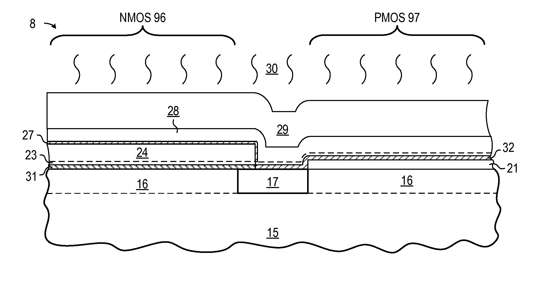
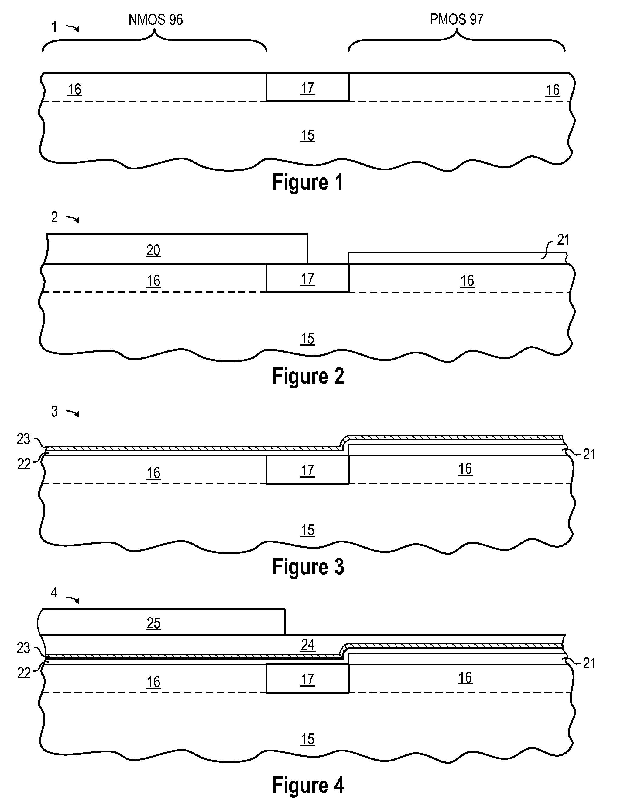
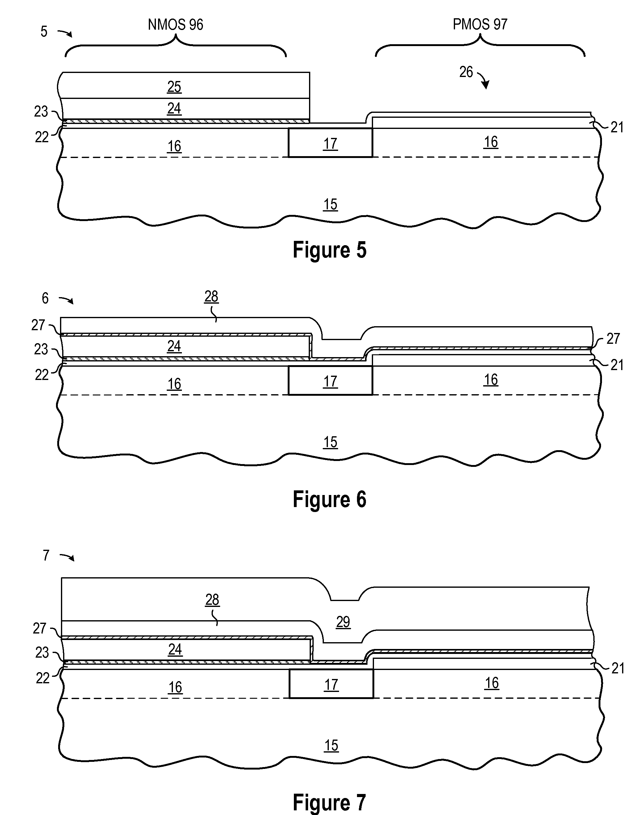
[0022]A method and apparatus are described for fabricating NMOS and PMOS transistors where each transistor includes a metal gate and a high-k gate dielectric that is doped with a species to shift the voltage threshold appropriately for the NMOS or PMOS device type. By forming separate NMOS and PMOS oxide capping layers on the high-k gate dielectric layer (e.g., hafnium dioxide) using a single patterned resist layer that is separated from the high-k gate dielectric layer by at least a first metal-based layer, the disclosed CMOS fabrication process provides separately doped gate dielectric layer while avoiding the problems created by putting resist in direct contact with the high-k gate dielectric layer. In addition, the disclosed integration scheme allows for resist rework, and results in the formation of a metal gate and high-k gate dielectric gate electrodes having substantially equal gate stack heights for the NMOS and PMOS devices. In an example process flow, a semiconductor wafe...


PUM


Abstract

A method and apparatus are described for fabricating single metal gate electrodes (35, 36) over a high-k gate dielectric layer (31, 32) that is separately doped in the PMOS and NMOS device areas (96, 97) by forming first capping oxide layer (23) with a first dopant species on a high-k gate dielectric layer (22) in at least the NMOS device area and also forming second capping oxide layer (27) with a second dopant species on a high-k gate dielectric layer (22) in at least the PMOS device area, where the first and second dopant species are diffused into the gate dielectric layer (22) to form a first fixed charge layer (31) in the PMOS device area of the high-k gate dielectric area and a second fixed charge layer (32) in the NMOS device area of the high-k gate dielectric area.

Description

BACKGROUND OF THE INVENTION[0001]1. Field of the Invention[0002]The present invention is directed in general to the field of semiconductor devices. In one aspect, the present invention relates to the fabrication of metal gate electrodes used in semiconductor devices.[0003]2. Description of the Related Art[0004]As the size and scaling of semiconductor device technology is reduced, aspects of device design and fabrication that previously gave rise to only second-order effects in long-channel devices can no longer be ignored. For example, the reduced scaling of channel length and gate oxide thickness in a conventional MOS transistor exacerbates problems of polysilicon gate depletion, high gate resistance, high gate tunneling leakage current and dopant (i.e., boron) penetration into the channel region of the device. As a result, CMOS technology is increasingly replacing silicon dioxide gate dielectrics and polysilicon gate conductors with high dielectric constant (high-k) dielectrics in...

Claims


Application Information

Patent Timeline
Patent Type & Authority Patents(United States)
IPC IPC(8): H01L21/8238
CPCH01L21/823807H01L21/823857H01L29/1054H01L29/4966H01L29/513H01L29/517
Inventor SCHAEFFER, JAMES K.LUCKOWSKI, ERIC D.
Owner TAIWAN SEMICON MFG CO LTD
Why Eureka
Try Eureka