Circuit pattern exposure method and mask

Active Publication Date: 2007-07-12
MICRON TECH INC
View PDF2 Cites 2 Cited by
  • Summary
  • Abstract
  • Description
  • Claims
  • Application Information

AI Technical Summary

Benefits of technology

[0012]It is an object of the present invention to reduce to the greatest extent possible the dimensional variation of not only the outmost pattern of concentrated circuit patterns, but also the patterns that are located around the outermost pattern.

Problems solved by technology

On the other hand, a modified illumination method such as oblique-incidence illumination has little effect on an isolated pattern in which diffracted light does not occur, and the depth of focus is not greatly extended.
Essentially, it has been difficult to simultaneously improve the exposure characteristics of both an isolated pattern and a highly concentrated pattern.
However, a method has been investigated in which a mask is used that is provided with mask patterns referred to as “auxiliary patterns” which do not themselves directly contribute to the formation of circuit patterns.
However, in the prior art, no consideration was given to the dimensional accuracy of the patterns that were inward from the outermost portion of the patterns when forming concentrated circuit patterns.

Method used


Image

  • Circuit pattern exposure method and mask
  • Circuit pattern exposure method and mask
  • Circuit pattern exposure method and mask

Examples


Embodiment Construction

[0026]This application is based upon and claims the benefit of priority from Japanese Patent Application No. 001357 / 06 filed on Jan. 6, 2006, the content of which is incorporated by reference.

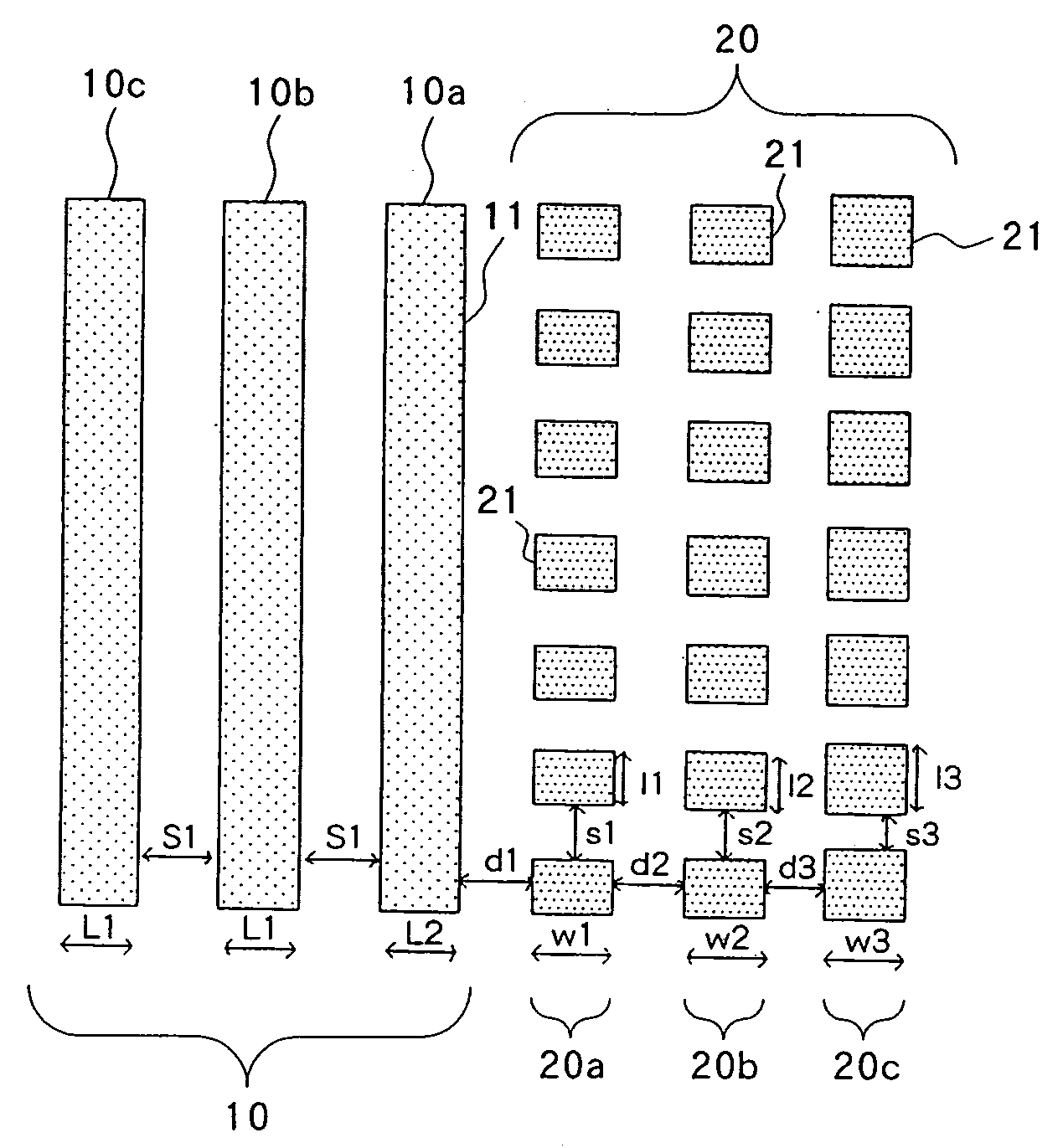
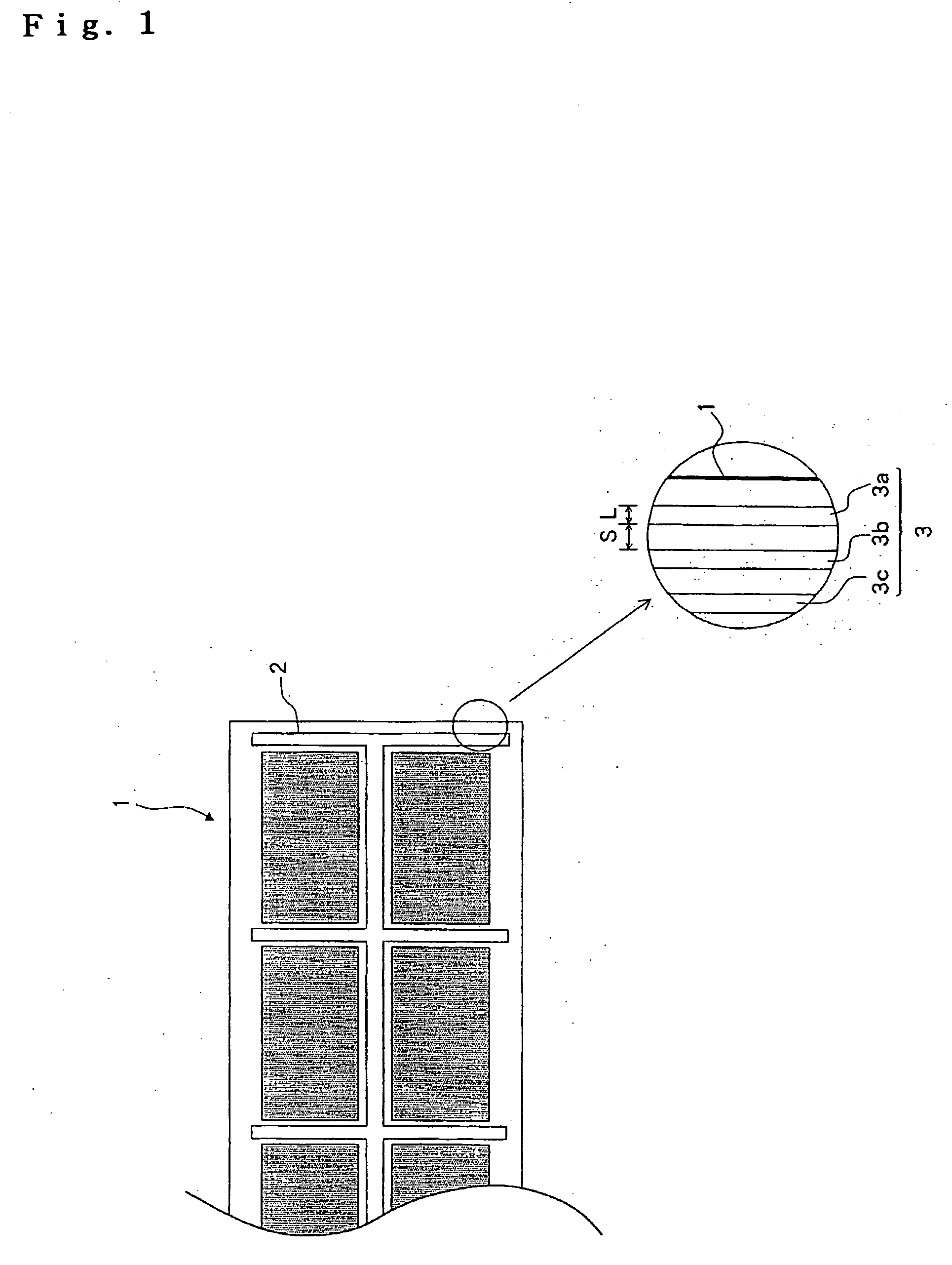
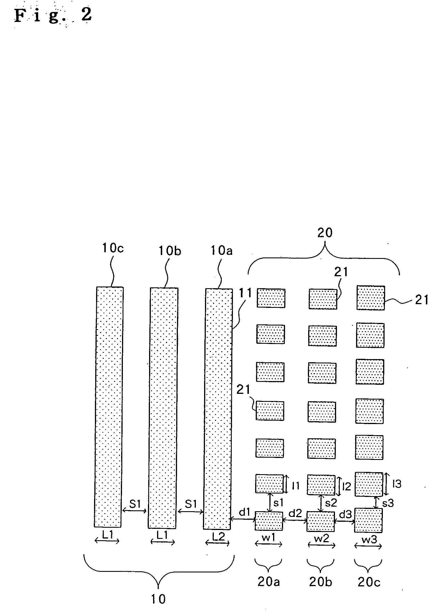
[0027]The circuit pattern exposure method of the present embodiment is directed to forming semiconductor circuit patterns of the type shown in the schematic view of FIG. 1. This semiconductor circuit pattern is circuit pattern 2 of DRAM (Dynamic Random Access Memory) 1. More specifically, this is an L / S (Line and Space) pattern in which a multiplicity of lines 3 of a prescribed line width are formed at a prescribed pitch. More particularly, FIG. 1 gives an enlarged view of only outermost line 3a and the two lines 3b and 3c that are arranged immediately inward from line 3a. The line width (L) of all lines 3 that includes lines 3a, 3b, and 3c is 100 nm, and the distance (S) between each of lines 3 is 100 nm.

[0028]Explanation next regards the exposure method of circuit pattern 2 shown in FIG. 1. S...


PUM


Abstract

A circuit pattern exposure method for irradiating illumination light onto a mask to transfer (offset) mask patterns that are formed in the mask to a semiconductor substrate, wherein the mask includes a plurality of main mask patterns that are arranged at a prescribed pitch and auxiliary mask patterns that are arranged outside the outermost main mask pattern and that are not to be transferred (offset) to the semiconductor substrate; the auxiliary mask patterns are provided with a first auxiliary mask row that is arranged adjacent to the outermost main mask pattern and a second auxiliary mask row that is arranged adjacent to the first auxiliary mask row; and the first auxiliary mask row and the second auxiliary mask row are arranged at a pitch that is narrower than the pitch of arrangement of the main mask patterns.

Description

BACKGROUND OF THE INVENTION[0001]1. Field of the Invention[0002]The present invention relates to a circuit pattern exposure method for forming circuit patterns on a semiconductor substrate and to a mask that is used in this method.[0003]2. Description of the Related Art[0004]With technological advances in the field of photolithography, micro circuit patterns can now be formed having a pitch that is less than one-half the optical wavelength of the exposure light. In particular, in the formation of a dense pattern such as a line / space pattern (hereinbelow abbreviated as “L / S pattern”) in which lines and spaces are repeated at a fixed pitch, sufficient depth of focus is obtained by the application of an oblique-incidence illumination method. The oblique-incidence illumination method is a method in which the vertical-incidence component of the illumination light that is irradiated onto a mask is cut such that the mask pattern is illuminated by the oblique-incidence component. In normal ...

Claims


Application Information

Patent Timeline
IPC IPC(8): G03F7/20G03F9/00G03F1/36G03F1/70H01L21/027
CPCG03F1/36G03F1/144
Inventor KOSA, NOBUEYASUZATO, TADAO
Owner MICRON TECH INC
Why Eureka
Try Eureka