Programmable Resistive RAM and Manufacturing Method

a technology of resistive ram and manufacturing method, which is applied in the direction of electrical apparatus, nanotechnology, semiconductor devices, etc., can solve the problems of processing compatibility problems, multi-function circuitry that combines multiple functions in this manner, and is associated with more complex fabrication

Active Publication Date: 2007-07-12
MACRONIX INT CO LTD
View PDF99 Cites 234 Cited by
  • Summary
  • Abstract
  • Description
  • Claims
  • Application Information

AI Technical Summary

Benefits of technology

[0016] Following the formation of the structures in the vias, various embodiments include the step of performing chemical mechanical polishing. Some embodiments perform chemical mechanical polishing non-selectively among the second dielectric layer, the third dielectric layer, the conductive lining, the dielectric lining, and the conductive structures. Some embodiments perform...

Problems solved by technology

However, multi-function circuitry that combines multiple functions in this manner is associated with more complex fabrication.
Even with multi-function integrated circuits that are designed f...

Method used


Image

  • Programmable Resistive RAM and Manufacturing Method
  • Programmable Resistive RAM and Manufacturing Method
  • Programmable Resistive RAM and Manufacturing Method

Examples


Embodiment Construction

[0034] Various embodiments are directed at a fast manufacturing method for memory, such as nonvolatile embedded memory implementing resistance device RAM. Examples of resistance device RAM are resistance memory (RRAM), polymer memory, and phase change memory (PCRAM).

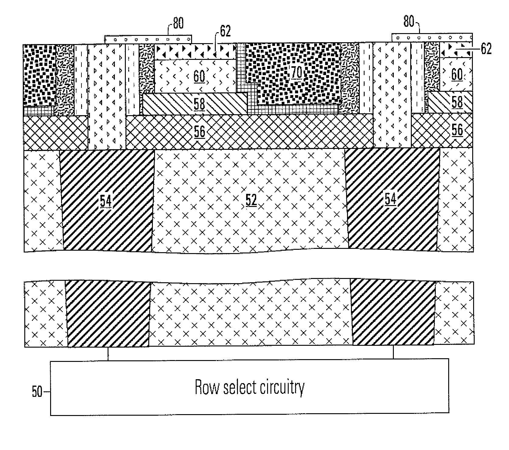
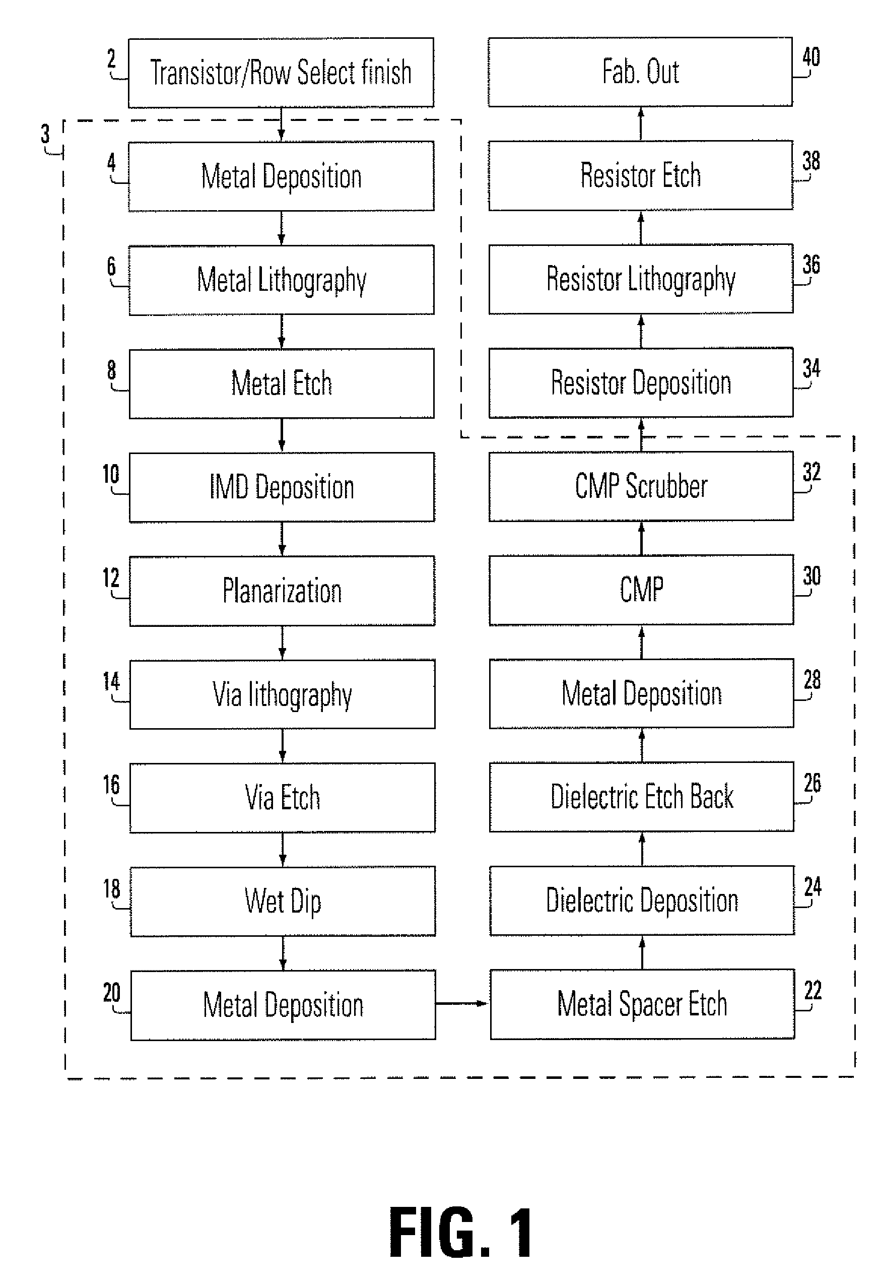
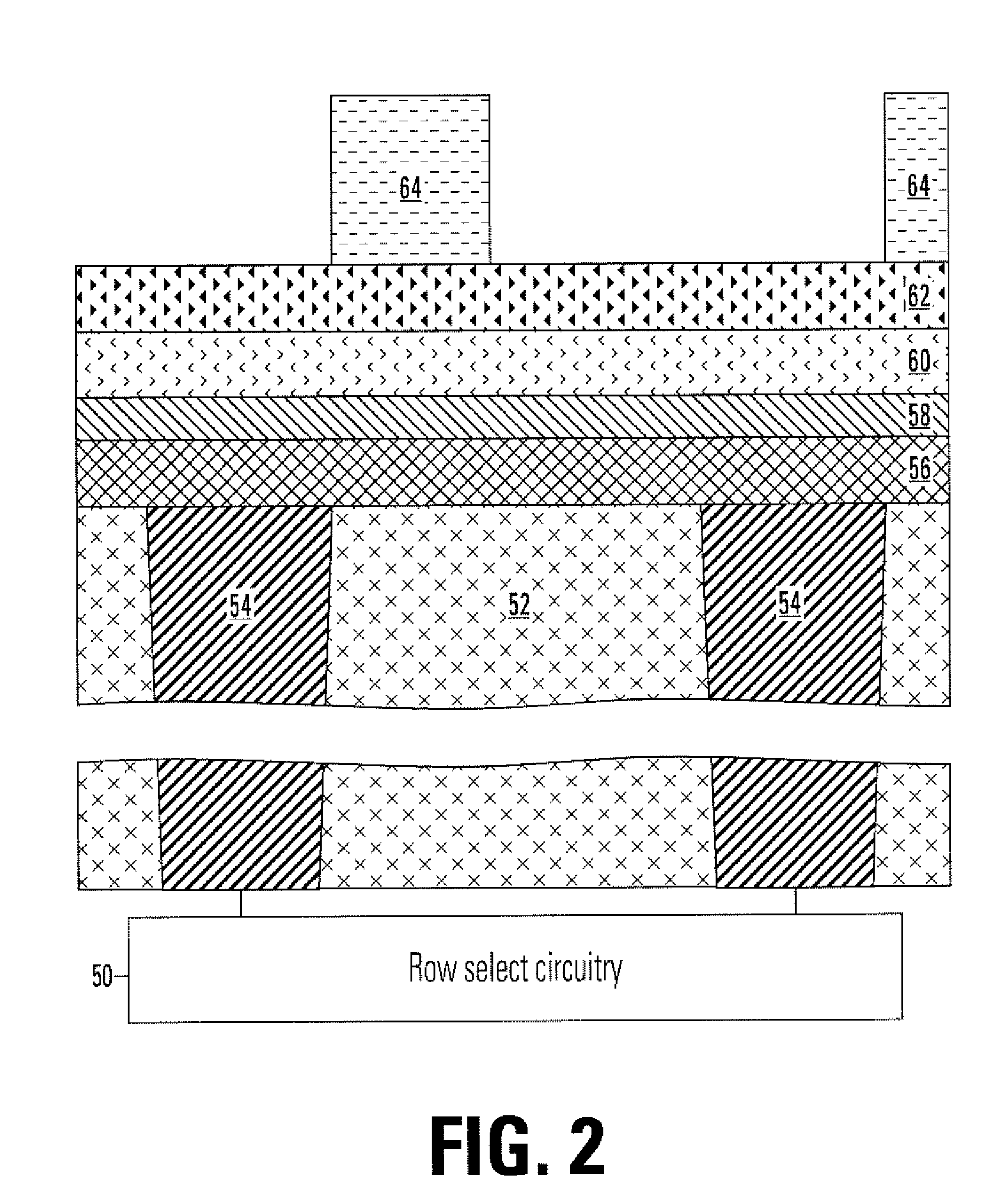
[0035]FIG. 1 is an example of a process flow to add programmable resistive memory to an integrated circuit. The nonvolatile resistance devices are designed to be the last process of fabrication. The resistive elements of the nonvolatile resistance devices are just formed on already fabricated electrodes. Before that, no contamination issues arise from resistance device in general fabrication of the remainder of the integrated circuit.

[0036] In transistor / row select finish 2, the mission circuitry of the integrated circuit other than the programmable resistive nonvolatile storage is fabricated, as well as the row access circuitry of the programmable resistive RAM. After transistor / row select finish 2, the programmable r...


PUM


Abstract

Integrated circuit nonvolatile memory uses programmable resistive elements. In some examples, conductive structures such as electrodes are prepared, and the programmable resistive elements are laid upon the prepared electrodes. This prevents contamination of the programmable resistive elements from previous fabrication steps.

Description

PRIORITY CLAIM [0001] This application claims the benefit of U.S. Provisional Application No. 60 / 757,275, filed 9 Jan. 2006 (MXIC 1679-1) by ChiaHua Ho entitled Method of Resistance Random Access Memory Device with Resistor-on-Electrodes Structure.BACKGROUND OF THE INVENTION [0002] 1. Field of the Invention [0003] The invention relates to integrated circuit nonvolatile memory. In particular, the invention relates to programmable resistive nonvolatile memory, such as phase change memory. [0004] 2. Description of Related Art [0005] Nonvolatile memory stores data without requiring a continuous supply of power. Thus, nonvolatile memory is useful in not only integrated circuits with nonvolatile storage as a primary purpose, but also integrated circuits with mission mode circuitry besides just data storage. [0006] However, multi-function circuitry that combines multiple functions in this manner is associated with more complex fabrication. If the multi-function integrated circuit was origi...

Claims


Application Information

Patent Timeline
IPC IPC(8): H01L21/336
CPCB82Y10/00H01L27/24H01L51/0591H01L51/0047H01L27/285H10B63/80H10N70/231H10N70/20H10N70/823H10N70/881H10N70/8828H10N70/8833H10N70/8836H10N70/011H10K19/202H10K85/215H10K10/50H10B63/00
Inventor HO, CHIAHUA
Owner MACRONIX INT CO LTD
Why Eureka
Try Eureka