Semiconductor device and method of manufacturing the same

a technology of semiconductors and semiconductors, applied in the direction of semiconductor devices, electrical devices, transistors, etc., can solve the problem of not completely removing the natural oxide film

Active Publication Date: 2007-07-12
RENESAS ELECTRONICS CORP
View PDF4 Cites 31 Cited by
  • Summary
  • Abstract
  • Description
  • Claims
  • Application Information

AI Technical Summary

Benefits of technology

[0012]The present invention is made in view of the problems described above. A first object of the present invention is to provide a method of manufacturing a semiconductor device, the method being capable of favorably removing a natural oxide film with a thickness that varies depending on its position, without overetching a sem...

Problems solved by technology

Furthermore, if the processing time period is set to meet the requirement for the thin...

Method used


Image

  • Semiconductor device and method of manufacturing the same
  • Semiconductor device and method of manufacturing the same
  • Semiconductor device and method of manufacturing the same

Examples


first embodiment

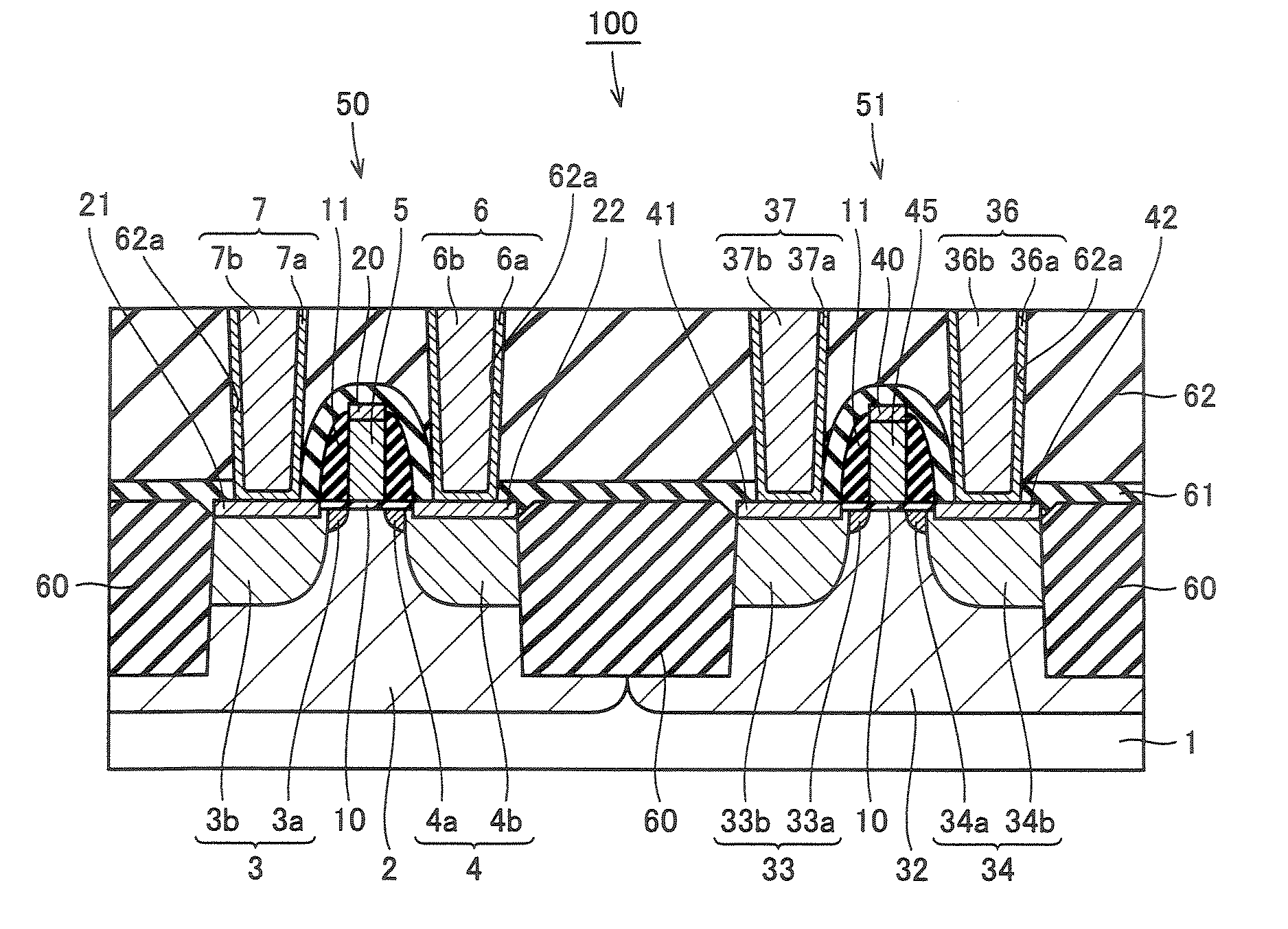
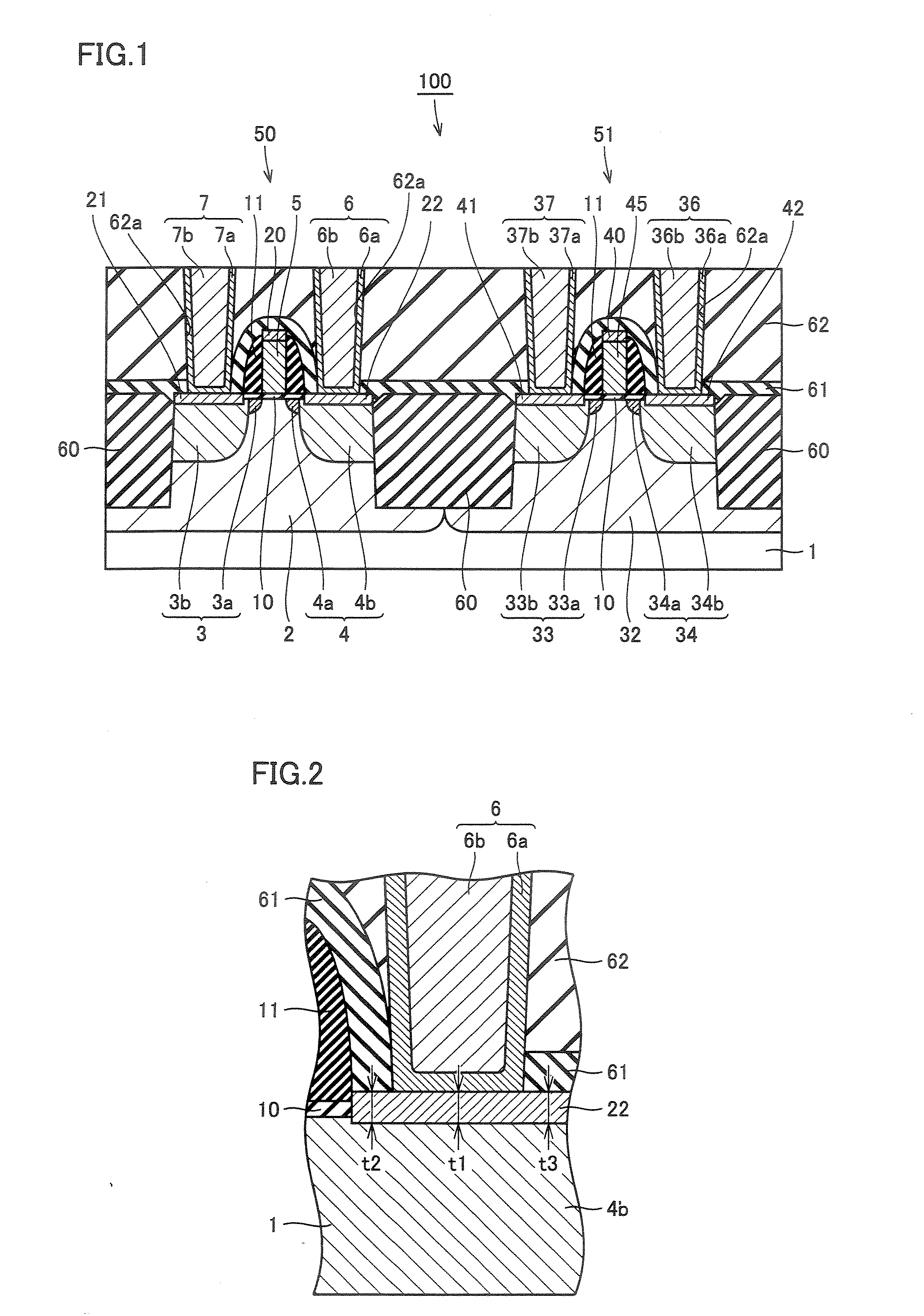
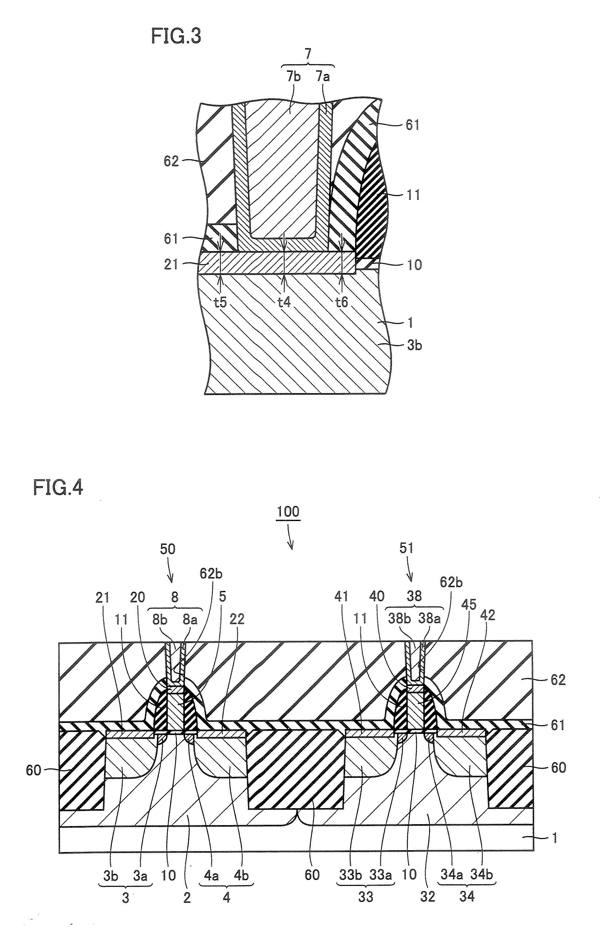
[0051]A semiconductor device and a method of manufacturing the same according to a first embodiment will hereinafter be described with reference to FIGS. 1 to 21. FIG. 1 is a cross section of a semiconductor device 100 according to the first embodiment. As shown in FIG. 1, semiconductor device 100 includes a semiconductor substrate 1, an isolated region 60 formed on a main surface of semiconductor substrate 1, an n-channel type Metal Oxide Semiconductor (MOS) transistor (hereinafter referred to as an nMOS transistor) 50 formed on the main surface of semiconductor substrate 1, and a p-channel type MOS transistor (hereinafter referred to as a pMOS transistor) 51 separated from nMOS transistor 50 by isolated region 60.

[0052]Semiconductor substrate 1 has a p-well region 2 and an n-well region 32 formed thereat, and nMOS transistor 50 is formed on a portion of the main surface of semiconductor substrate 1 where p-well region 2 is located, while pMOS transistor 51 is formed on a portion o...

second embodiment

[0103]A semiconductor device according to a second embodiment will hereinafter be described with reference to FIGS. 22 to 30. There may be a case where a configuration identical to or corresponding to that shown in FIGS. 1 to 21 described above, is denoted by the same reference character and the description thereof is not repeated.

[0104]FIG. 22 is a cross section of an nMOS transistor 150 in the semiconductor device according to the second embodiment. As shown in FIG. 22, p-well region 2 is formed in semiconductor substrate 1, and nMOS transistor 150 is formed at a portion of the main surface of semiconductor substrate 1 where well region 2 is located.

[0105]The nMOS transistor 150 is formed on the portion of the main surface of semiconductor substrate 1 where p-well region 2 is located, and includes insulating film 10 formed of a silicon oxide film, for example, gate electrode 5 formed on insulating film 10, and impurity regions 3 and 4 formed on portions of the main surface of semi...


PUM


Abstract

A method of manufacturing a semiconductor device according to the present invention includes the steps of introducing first impurities of a first conductivity type into a main surface of a semiconductor substrate 1 to form a first impurity region, introducing second impurities of a second conductivity type to form a second impurity region, forming a first nickel silicide film on the first impurity region and forming a second nickel silicide film on the second impurity region, removing an oxide film formed on each of the first and second nickel silicide films by using a mixed gas having an NH3 gas and a gas containing a hydrogen element mixed therein, and forming a first conducting film on the first nickel silicide film and forming a second conducting film on the second nickel silicide film, with the oxide film removed.

Description

BACKGROUND OF THE INVENTION[0001]1. Field of the Invention[0002]The present invention relates to a semiconductor device and a method of manufacturing the same.[0003]2. Description of the Background Art[0004]When there is manufactured a semiconductor device having a metal film formed on a main surface of a semiconductor substrate, a natural oxide film tends to be formed on a surface of the metal film. Accordingly, when a contact portion or the like is formed on the metal film having the natural oxide film formed thereon, the natural oxide film blocks conduction between the contact portion and the metal film, which inevitably exerts a substantial influence on a characteristic of the semiconductor device to be manufactured. Accordingly, there have conventionally been proposed various types of cleaning methods, processing devices and the like for removing the natural oxide film formed on the metal film and the main surface of the semiconductor substrate.[0005]For example, Japanese Paten...

Claims


Application Information

Patent Timeline
IPC IPC(8): H01L21/265
CPCH01L21/0206H01L21/02063H01L21/28518H01L21/76814H01L21/76816H01L21/76843H01L29/7833H01L21/823418H01L21/823443H01L21/823475H01L29/665H01L29/6659H01L21/76895H01L21/76897
Inventor ICHINOSE, KAZUHITOYUTANI, AKIE
Owner RENESAS ELECTRONICS CORP
Why Eureka
Try Eureka