Exposure apparatus and device manufacturing method
- Summary
- Abstract
- Description
- Claims
- Application Information
AI Technical Summary
Benefits of technology
Problems solved by technology
Method used
Image

Examples
first embodiment
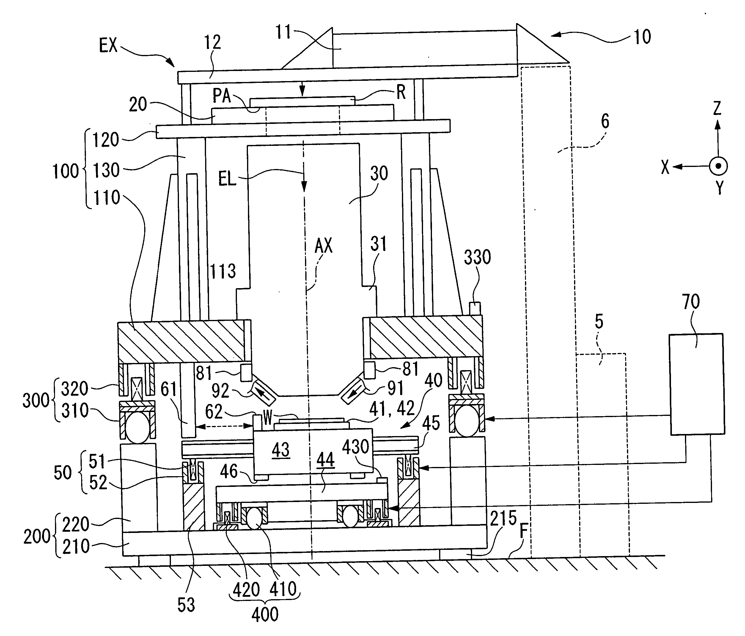
[0062]FIG. 1 is a schematic diagram showing the configuration of an exposure apparatus EX according to the invention. The exposure apparatus EX is a step-and-scan type scanning exposure system, so-called, a scanning stepper which, while moving a reticle (mask) R and a wafer (substrate, object) W in a one-dimensional direction in sync, transfers a circuit pattern PA formed on the reticle R onto each shot area on the wafer. W via a proyection optical system 30.
[0063] In the following explanation, the direction coincident with the optical axis AX of the projection optical system 30 is taken to be the Z-axis direction, the direction of synchronized movement of the reticle R and wafer W within the plane perpendicular to the Z-axis direction (the scanning direction) is the Y-axis direction, and the direction perpendicular to the Z-axis direction and to the Y-axis direction (the non-scanning direction) is the X-axis direction. The directions about the X axis, Y axis, and Z axis are respect...
second embodiment
[0133] Next, an exposure apparatus of this invention is explained, with reference to the drawings. Component portions which are the same as or equivalent to those in the embodiment explained above are assigned the same symbols, and explanations are omitted or simplified.
[0134]FIG. 5 shows the configuration of an exposure apparatus EX2 of the second embodiment of the invention. The exposure apparatus EX2 of this embodiment comprises an abnormality detector 71. The abnormality detector 71 detects errors occurring in each of the controllers constituting the control device 70, and detects whether an abnormality has occurred in the exposure apparatus EX2.
[0135] Here, an abnormality is an operation which may result in a collision between the projection optical system 30, liquid supply device 91, liquid recovery device 92, or other members (opposing members) positioned above the wafer W, and the wafer table 42, wafer W, or other members (objects) positioned below the projection optical sy...
PUM
 Abstract
Description
Claims
Application Information
 - Generate Ideas
- Intellectual Property
- Life Sciences
- Materials
- Tech Scout
- Unparalleled Data Quality
- Higher Quality Content
- 60% Fewer Hallucinations
Browse by: Latest US Patents, China's latest patents, Technical Efficacy Thesaurus, Application Domain, Technology Topic, Popular Technical Reports.
© 2025 PatSnap. All rights reserved.Legal|Privacy policy|Modern Slavery Act Transparency Statement|Sitemap|About US| Contact US: help@patsnap.com