Semiconductor chip

Active Publication Date: 2007-07-19
QUALCOMM INC
View PDF63 Cites 75 Cited by
  • Summary
  • Abstract
  • Description
  • Claims
  • Application Information

AI Technical Summary

Problems solved by technology

Moreover, in the flip-chip technology, multiple bumps can be formed on the chip for connecting the chip to a substrate.
Moreover, the testing probes may contact the bumps repeatedly during the testing step.
As a result, the bumps are subje

Method used


Image

  • Semiconductor chip
  • Semiconductor chip
  • Semiconductor chip

Examples


embodiment i

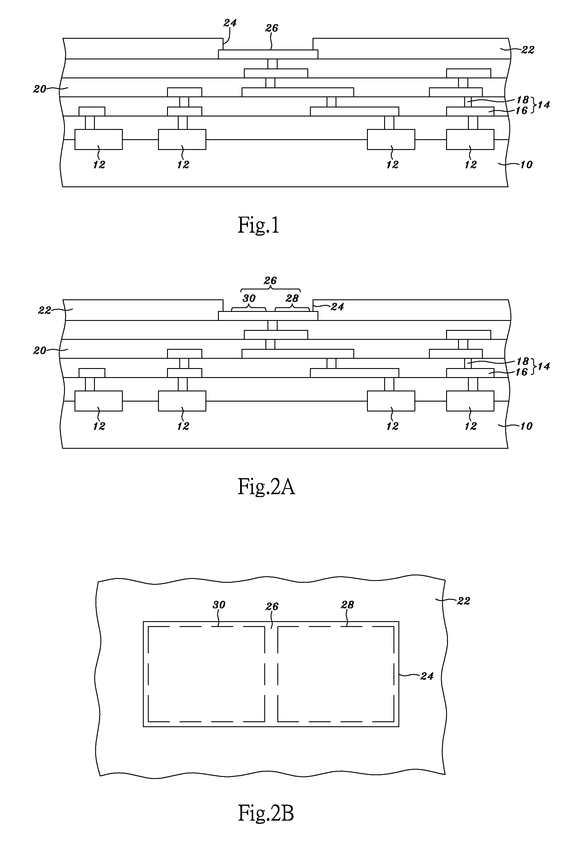
[0063] Refer to FIG. 2A and FIG. 2B respectively a sectional view and a partial top view schematically showing a wafer. As shown in FIG. 2A and FIG. 2B, the pad 26 has a testing area 28 for electrical testing and a bond area 30 to be electrically connected to an external system, such as a printed circuit board, a ball grid array (BGA) substrate, a mother board, a glass substrate, a ceramic substrate, a flexible circuit film, a TAB carrier, a semiconductor wafer, or a semiconductor chip. The examples for the external system in this embodiment may be employed to any below-mentioned external system depicted in other embodiments.

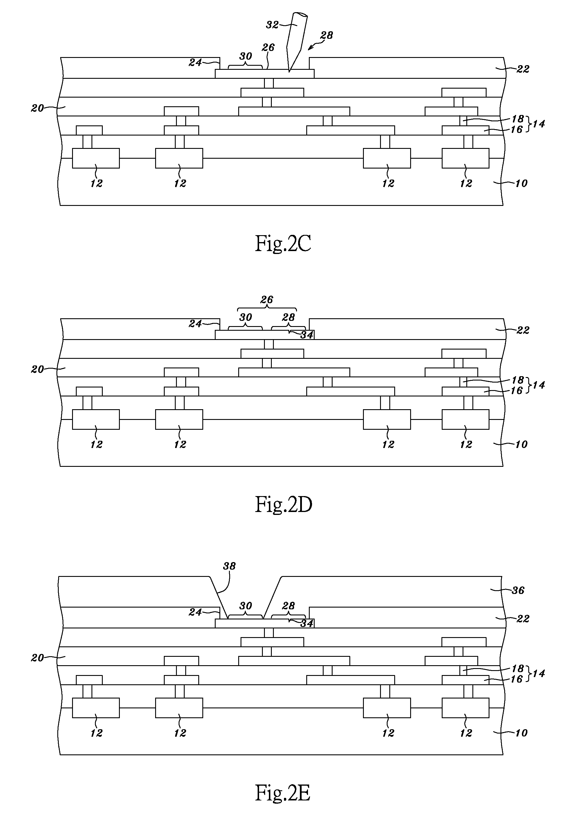
[0064] Refer to FIG. 2C. During a step of testing, a testing probe 32 contacts with the testing area 28 of a pad 26 for electrical testing. Refer to FIG. 2D. After the step of testing, the testing probe 32 is removed, and a probe mark 34 is left on the testing area 28. Refer to FIG. 2E. A patterned polymer layer 36 is formed over the passivation layer 22 and th...

embodiment ii

[0072] Refer to FIG. 3A. After the progress shown in FIG. 2D, an adhesion / barrier layer 40 having a thickness of between 0.02 and 2 μm is formed over the pad 26 and the passivation layer 22. Next, a seed layer 42 is formed over the adhesion / barrier layer 40. Refer to Embodiment I for the detailed technical description of the adhesion / barrier layer 40 and the seed layer 42.

[0073] Refer to FIG. 3B. Next, a photoresist layer 44 is formed over the seed layer 42, and the photoresist layer 44 is patterned to form a photoresist-layer opening 46 to expose the seed layer 42 over the bond area 30 of the pad 26, wherein a 1× stepper or a 1× scanner is used to expose the photoresist layer 44 during forming the photoresist-layer opening 46. Refer to FIG. 3C. Next, a metal layer 48 having a thickness of between 1 and 200 μm (e.g. a thickness of between 20 and 120 μm) is formed over the seed layer 42 exposed by the photoresist-layer opening 46. Refer to Embodiment I for the detailed technical des...

embodiment iii

[0077] This embodiment exemplifies the application of the present invention to a redistribution layer (RDL). Refer to FIG. 4A. After the progress shown in FIG. 2G, a first photoresist layer 52 is formed over the seed layer 42, and the first photoresist layer 52 is patterned to form a first-photoresist-layer opening 54 to expose the seed layer 42 over the bond area 30 of the pad 26 and expose the seed layer 42 over a portion of the patterned polymer layer 36 extending from the bond area 30, wherein a 1× stepper or a 1× scanner is used to expose the first photoresist layer 52 during forming the first-photoresist-layer opening 54. The first-photoresist-layer opening 54 has a dimension W1 of between 60 μm and 10 mm.

[0078] Refer to FIG. 4B. Next, a first metal layer 56 having a thickness of between 1 and 30 μm is electroplated on the seed layer 42 exposed by the first-photoresist-layer opening 54. The first metal layer 56 may be a single layer made of gold, copper, nickel, aluminum, sil...


PUM


Abstract

A semiconductor chip comprises a metal pad exposed by an opening in a passivation layer, wherein the metal pad has a testing area and a bond area. During a step of testing, a testing probe contacts with the testing area for electrical testing. After the step of testing, a polymer layer is formed on the testing area with a probe mark created by the testing probe. Alternatively, a semiconductor chip comprises a testing pad and a bond pad respectively exposed by two openings in a passivation layer, wherein the testing pad is connected to the bond pad. During a step of testing, a testing probe contacts with the testing pad for electrical testing. After the step of testing, a polymer layer is formed on the testing pad with a probe mark created by the testing probe.

Description

[0001] This application claims priority to U.S. provisional application No. 60 / 597,493, filed on Dec. 5 2005, which are herein incorporated by reference in their entirety.BACKGROUND OF THE INVENTION [0002] 1. Field of the Invention [0003] The present invention relates to a semiconductor chip, particularly to a semiconductor chip, wherein a polymer layer is used to cover a probe mark. [0004] 2. Brief Description of the Related Art [0005] Information products are playing important roles in today's competitive society. With the evolution of the information products and the introduction of the concept of integrating various circuit designs, the latest single chip, generally, provides more functions than the former one. After integration, the dimension of the circuits is reduced and the majority of the signals are being transmitted within a single chip. As a result, paths for transmitting signals are reduced and the performance of the chip is improved. [0006] Moreover, in the flip-chip t...

Claims


Application Information

Patent Timeline
IPC IPC(8): H01L23/58
CPCH01L22/32H01L24/03H01L24/05H01L24/11H01L24/12H01L24/94H01L2224/0231H01L2224/03912H01L2224/05018H01L2224/05557H01L2224/05558H01L2224/05599H01L2224/05624H01L2224/05644H01L2224/05655H01L2224/05666H01L2224/05681H01L2224/1147H01L2224/1191H01L2224/11912H01L2224/13021H01L2224/13022H01L2224/13024H01L2224/13099H01L2224/13111H01L2224/13139H01L2224/13144H01L2224/13147H01L2224/13155H01L2224/13164H01L2224/13169H01L2224/16H01L2224/274H01L2924/01007H01L2924/01011H01L2924/01013H01L2924/01014H01L2924/01015H01L2924/01018H01L2924/01022H01L2924/01027H01L2924/01028H01L2924/01029H01L2924/01046H01L2924/01047H01L2924/0105H01L2924/01073H01L2924/01074H01L2924/01075H01L2924/01078H01L2924/01079H01L2924/01082H01L2924/014H01L2924/04941H01L2924/04953H01L2924/05042H01L2924/09701H01L2924/10329H01L2924/19041H01L2924/19042H01L2924/19043H01L2224/0558H01L2924/01006H01L2924/01019H01L2924/01023H01L2924/01024H01L2924/01033H01L2924/01044H01L2924/01045H01L2924/00014H01L2224/05027H01L2224/05572H01L2224/0401H01L2224/02166H01L2224/05553H01L2924/1305H01L2924/00H01L2924/15787H01L2924/15788H01L2224/0392
Inventor LIN, MOU-SHIUNGYEN, HUEI-MEICHOU, CHIU-MINGLO, HSIN-JUNGCHEN, KE-HUNG
Owner QUALCOMM INC
Why Eureka
Try Eureka