Pre-gate dielectric process using hydrogen annealing

a technology of pre-gate dielectric and hydrogen annealing, which is applied in the direction of semiconductor/solid-state device manufacturing, basic electric elements, electric apparatus, etc., can solve the problems of increasing leakage current, unexpected (adverse) effects of devices formed, and cost, so as to improve performance and reliability, and improve the performance of devices in other regions.

Active Publication Date: 2007-07-19
TAIWAN SEMICON MFG CO LTD
View PDF25 Cites 13 Cited by
  • Summary
  • Abstract
  • Description
  • Claims
  • Application Information

AI Technical Summary

Benefits of technology

[0012] The advantageous features of the preferred embodiments of the present invention includes restricting hydrogen annealing in desired regions, so that device performance in other re

Problems solved by technology

However, when the EOT of a MOS device is reduced, leakage current often increases.
The incorporation of nitrogen into the

Method used


Image

  • Pre-gate dielectric process using hydrogen annealing
  • Pre-gate dielectric process using hydrogen annealing
  • Pre-gate dielectric process using hydrogen annealing

Examples


Embodiment Construction

[0015] The making and using of the presently preferred embodiments are discussed in detail below. It should be appreciated, however, that the present invention provides many applicable inventive concepts that can be embodied in a wide variety of specific contexts. The specific embodiments discussed are merely illustrative of specific ways to make and use the invention, and do not limit the scope of the invention.

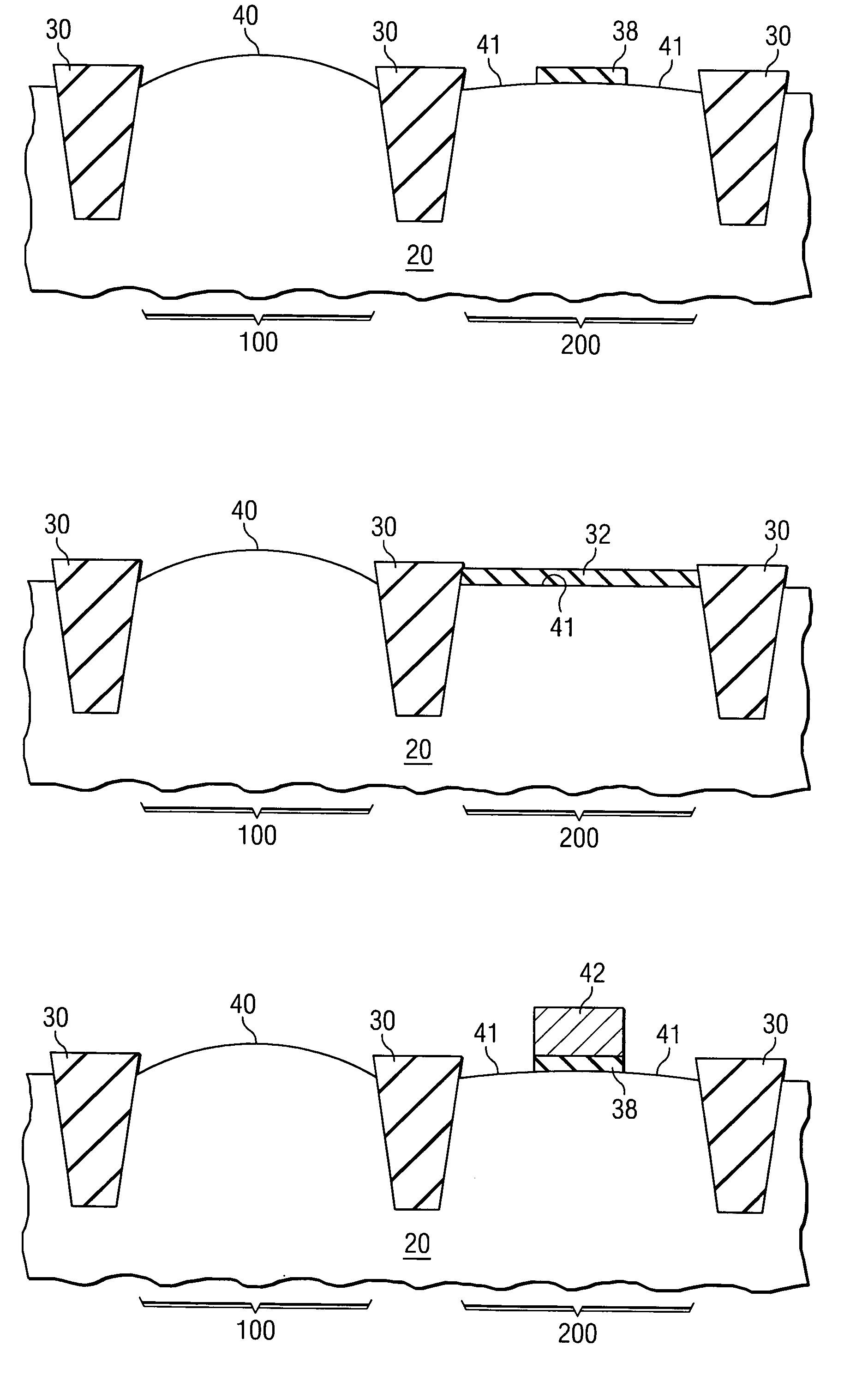
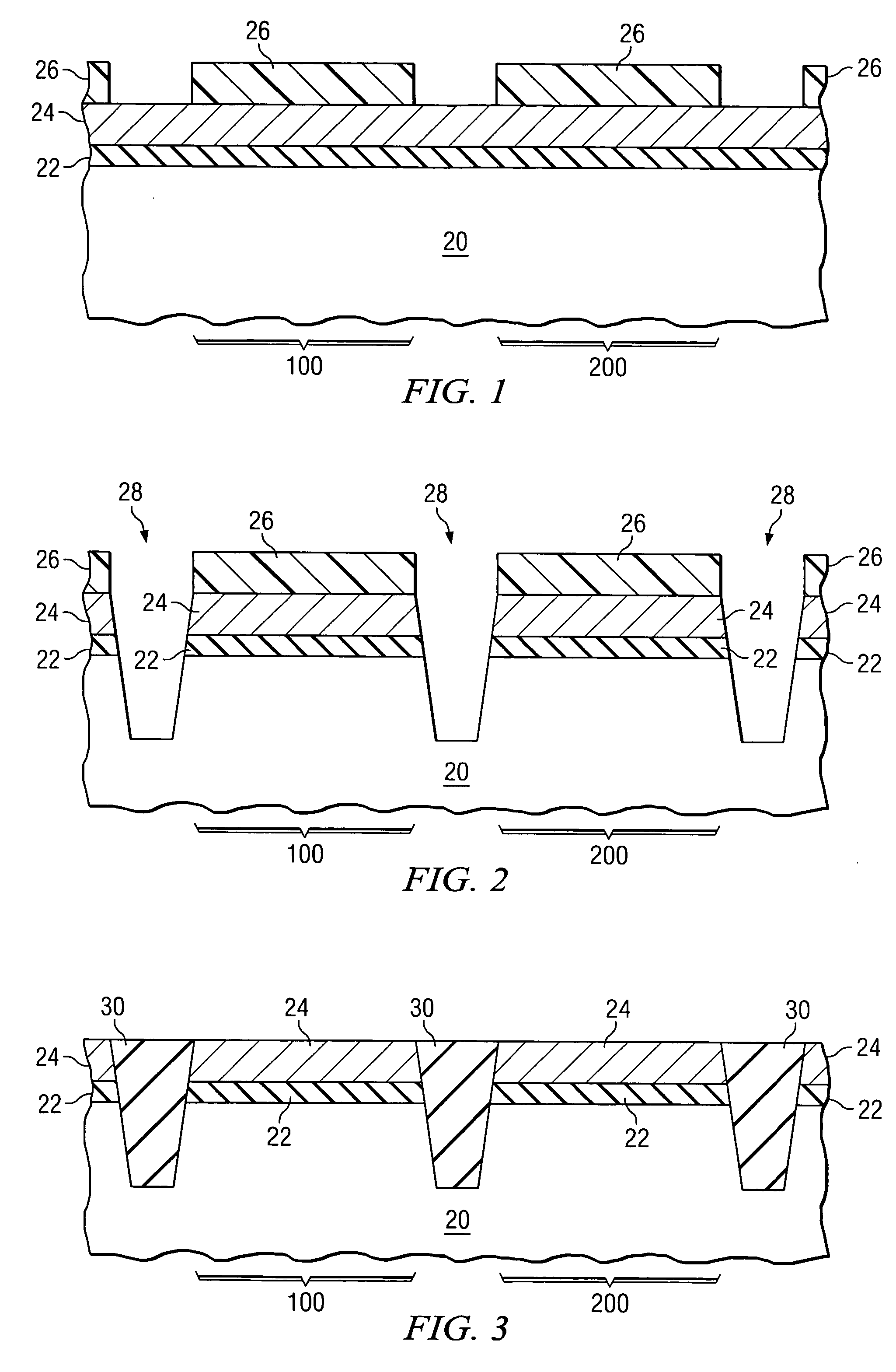
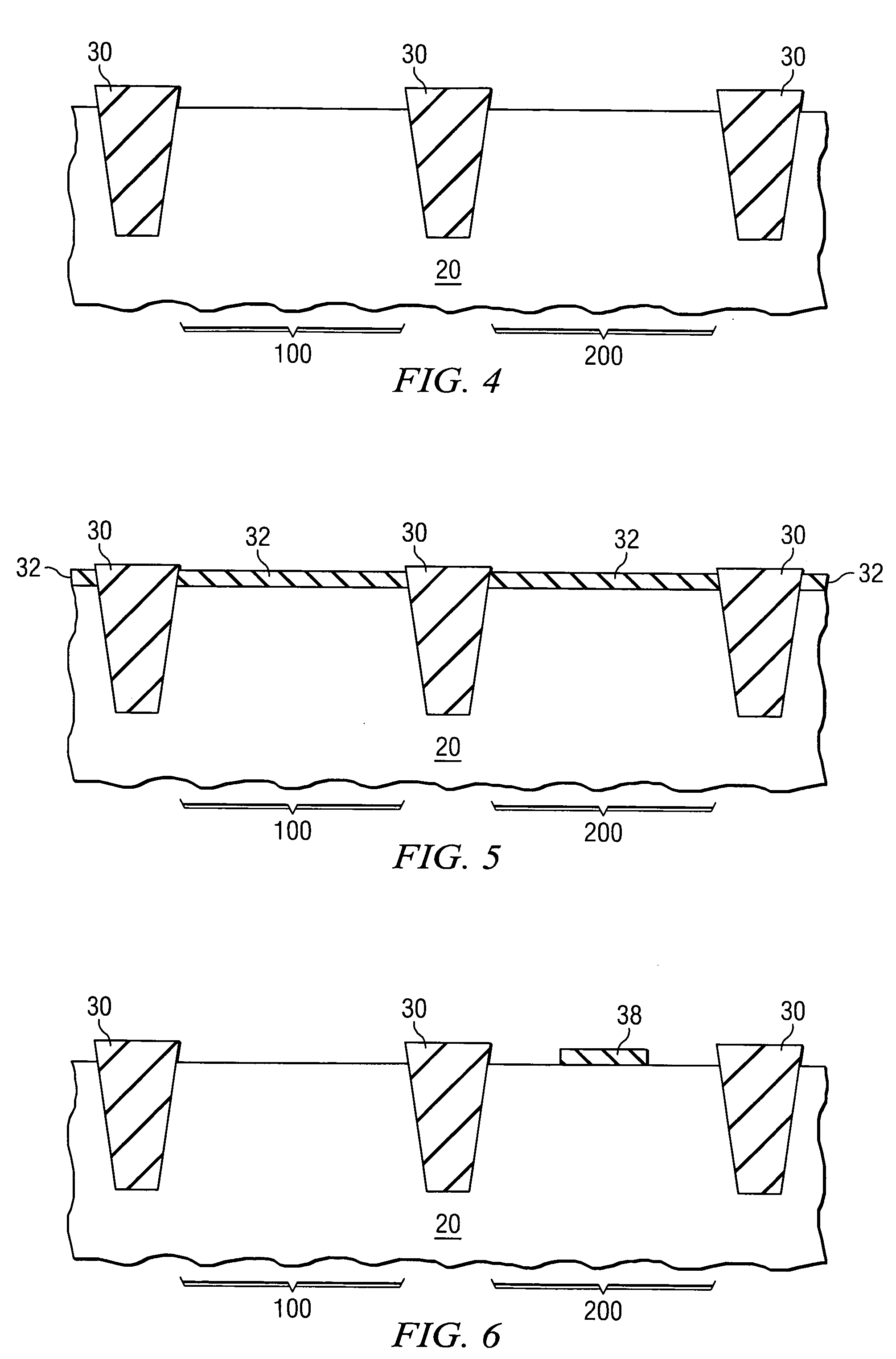
[0016]FIGS. 1 through 9 illustrate intermediate stages in the manufacture of the preferred embodiments of the present invention. Throughout the various views and illustrative embodiments of the present invention, like reference numbers are used to designate like elements. Referring to FIG. 1, a substrate 20 and a starting structure for the formation of shallow trench isolation regions are shown. In the preferred embodiment, the substrate 20 is a bulk silicon substrate. In other embodiments, the substrate 20 comprises silicon, germanium, carbon, and combinations thereof. In ...


PUM


Abstract

The preferred embodiment of the present invention provides a novel method of forming MOS devices using hydrogen annealing. The method includes providing a semiconductor substrate including a first region and a second region, forming at least a portion of a first MOS device covering at least a portion of the first active region, performing a hydrogen annealing in an ambient containing substantially pure hydrogen on the semiconductor substrate. The hydrogen annealing is performed after the step of the at least a portion of the first MOS device is formed, and preferably after a pre-oxidation cleaning. The method further includes forming a second MOS device in the second active region after hydrogen annealing. The hydrogen annealing causes the surface of the second active region to be substantially rounded, while the surface of the first active region is substantially flat.

Description

CROSS-REFERENCE TO RELATED APPLICATIONS [0001] This application relates to the following commonly assigned U.S. patent application Ser. No. ______ Docket No. TSM05-0196, entitled “Diffusion Topography Engineering for High Performance CMOS Fabrication,” which patent application is incorporated herein by reference. TECHNICAL FIELD [0002] This invention relates generally to structure and fabrication methods of metal-oxide-semiconductor (MOS) devices, and more particularly to device mobility improvement through pre-gate processes. BACKGROUND [0003] With scaling of VLSI circuits, more devices are put into a chip. This not only requires the shrinking of the device size, but it also puts higher requirements on each component of the semiconductor devices. [0004] Reducing equivalent oxide thickness (EOT) of a gate dielectric is important for a metal-oxide-semiconductor (MOS) device to have high performance. Many methods have been explored to reduce the EOT of the gate dielectric. However, wh...

Claims


Application Information

Patent Timeline
IPC IPC(8): H01L21/8234H01L21/336
CPCH01L21/823807H01L21/823828H01L21/823857
Inventor TEO, JOCELYN WEI-YEECHEN, CHI-CHUNCHEN, SHIH-CHANG
Owner TAIWAN SEMICON MFG CO LTD
Why Eureka
Try Eureka