Semiconductor device, interposer chip and manufacturing method of semiconductor device

a manufacturing method and semiconductor technology, applied in semiconductor devices, semiconductor/solid-state device details, electrical devices, etc., can solve problems such as defective units, failure of bonding wires, and inability to easily contact the burr of the end face of microcomputer chips, etc., to achieve stably the effect of performan

Active Publication Date: 2007-07-26
RENESAS ELECTRONICS CORP
View PDF3 Cites 76 Cited by
  • Summary
  • Abstract
  • Description
  • Claims
  • Application Information

AI Technical Summary

Benefits of technology

[0028]Yet another manufacturing method of a semiconductor device concerning this invention is a manufacturing method of a semiconductor device which manufactures a semiconductor device with which a plurality of chips were stacked over a front surface of a wiring substrate, wherein a plurality of first electrodes are arranged along one side of the wiring substrate; a plurality of second electrodes are arranged along one side of respective chips; the chips are stacked so that the second electrodes of respective chips may be exposed, shifting predetermined distance; each second electrode is connected to a corresponding first electrode via a bonding wire; a mold which has rectangular parallelepiped-like interior space, an inlet formed in one corner of this interior space, and an exhaust port formed in a corner which faces with this inlet is prepared; and one side of the wiring substrate is turned in the same direction as one side of a bottom of the interior space, the semiconductor device is arranged in the interior space, liquid resin for sealing is injected from the inlet, and the interior space is made to fill up with and cure the liquid resin for sealing. Therefore, as big inflow pressure cannot be applied to a chip, liquid resin can be made to be able to flow into the space between a chip and a wiring substrate, and it can be prevented that a void is made in the space between a chip and a wiring substrate, or a chip is removed.
[0029]Still another semiconductor device concerning this invention is a semiconductor device with which a first-Nth (however, N is three or more integers) chips were stacked over a front surface of a wiring substrate, wherein a plurality of first electrodes are arranged along one side of the wiring substrate; a plurality of second electrodes are arranged along a side opposite to the one side of the wiring substrate; a plurality of third electrodes are arranged along each one side at the side of the first electrodes of the first to N−1th chips; the first to N−1th chips can be shifted a predetermined distance, and are stacked so that the third electrodes of the first to N−1th chip may be exposed; a plurality of fourth electrodes are arranged along one side at a side of the second electrodes of the Nth chip; the Nth chip is arranged over N−1th chip so that the Nth chip and the N−1th chip may exist at least between the fourth electrodes and a front surface of the wiring substrate; each third electrode is connected to a corresponding first electrode via a bonding wire; and each fourth electrode is connected to a corresponding second electrode via a bonding wire. Therefore, since a plurality of chips exist under a fourth electrode, when doing bonding of the wire to a fourth electrode, it can prevent that the Nth chip deforms greatly according to the load applied to a fourth electrode, and wire bonding can be performed stably.

Problems solved by technology

However, in a conventional semiconductor device, there was a problem that the bonding wire struck and taken down from the microcomputer chip to the wiring substrate contacted the electrically conductive burr exposed to the end face of a microcomputer chip, and malfunction occurred.
Therefore, the bonding wire cannot contact the burr of the end face of a microcomputer chip easily.
However, when such a semiconductor device was stored in a mold and liquid resin for sealing was injected into a mold, the bonding wire deformed with the pressure into which liquid resin flows, and there was a problem that bonding wires contacted and a defective unit was generated.

Method used


Image

  • Semiconductor device, interposer chip and manufacturing method of semiconductor device
  • Semiconductor device, interposer chip and manufacturing method of semiconductor device
  • Semiconductor device, interposer chip and manufacturing method of semiconductor device

Examples


embodiment 1

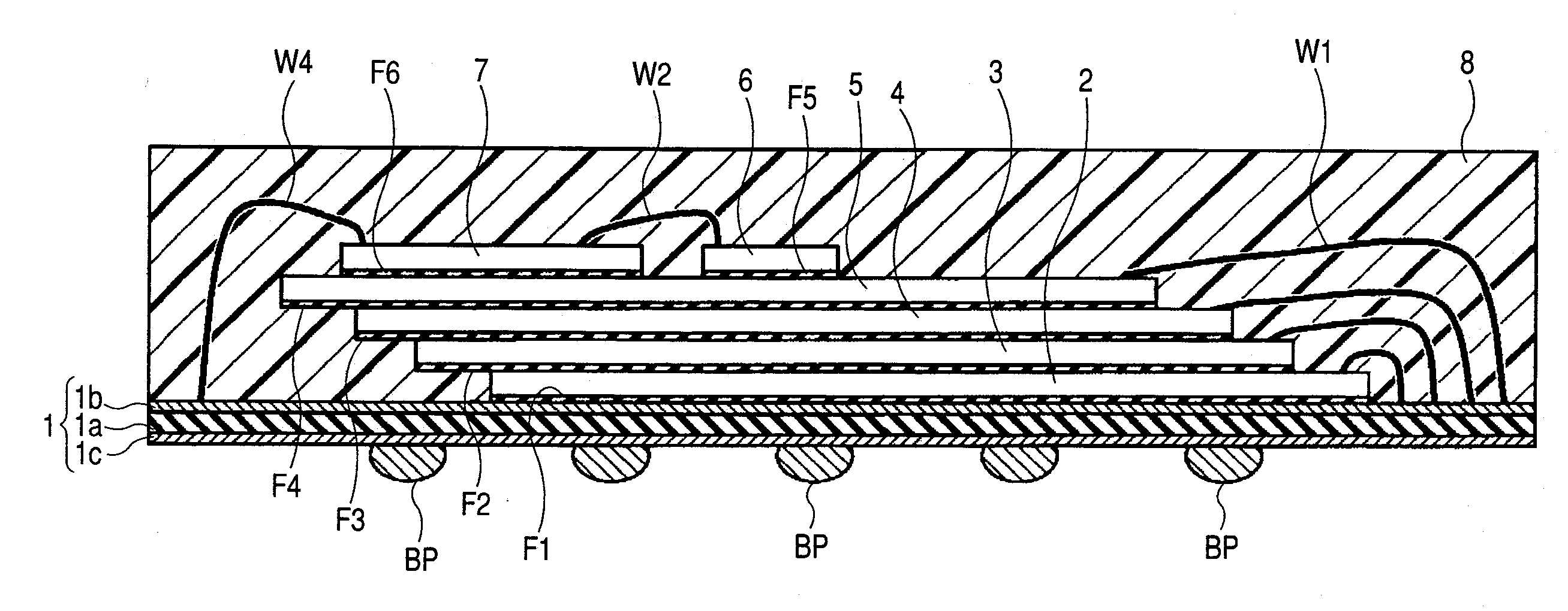
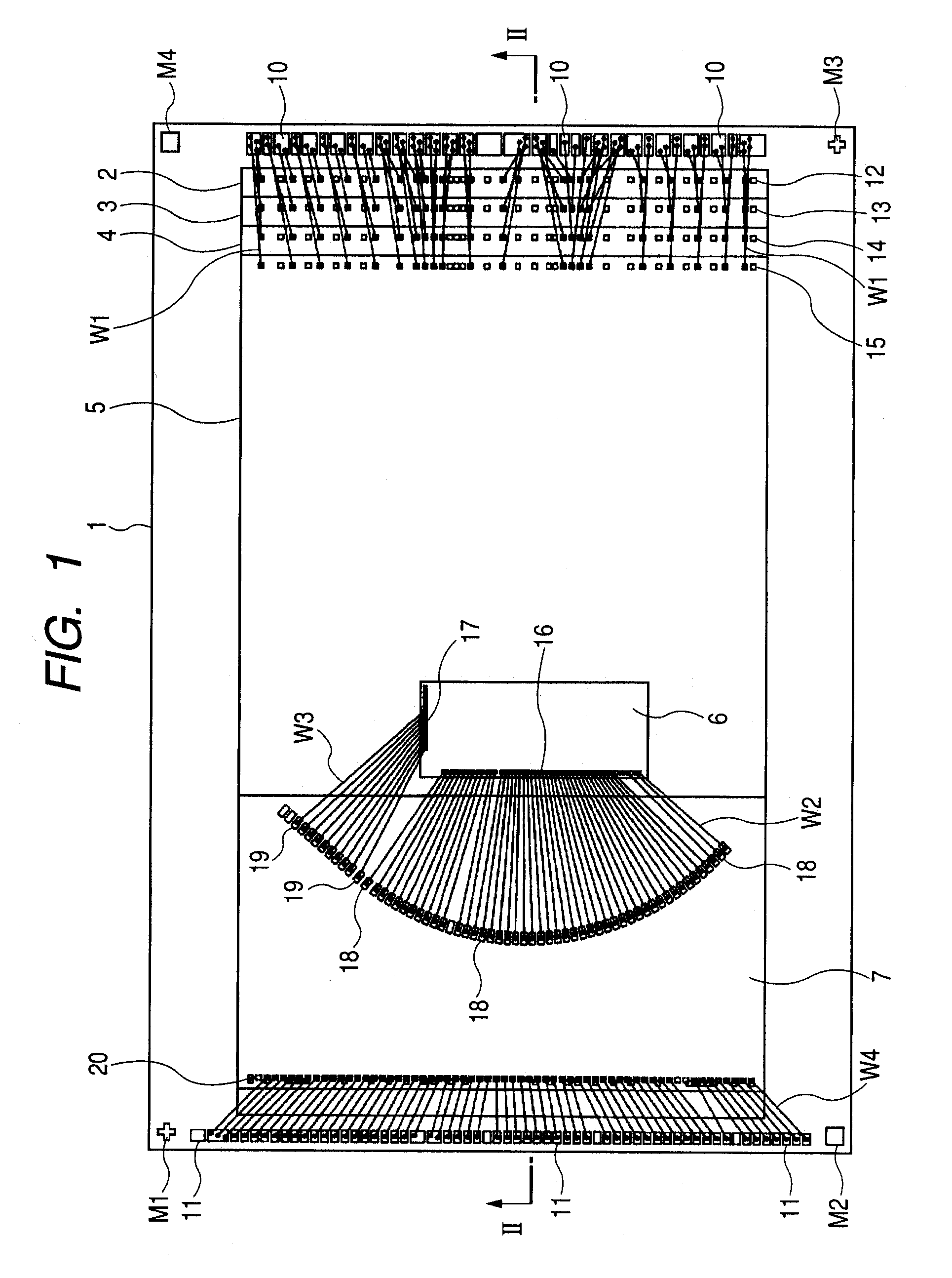
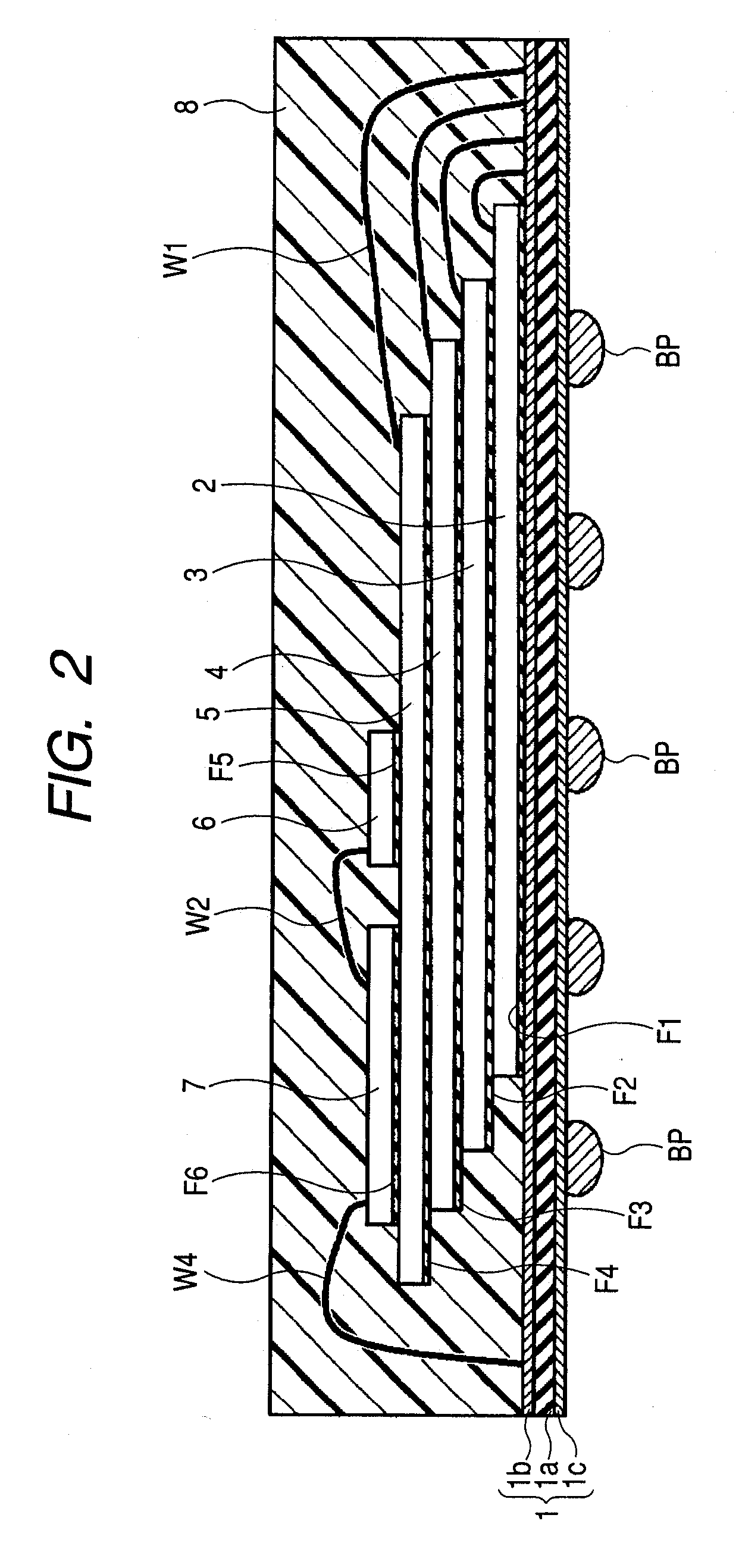
[0050]FIG. 1 is a plan view showing the structure of the semiconductor device by this embodiment of the invention 1, and FIG. 2 is an II-II line cross-sectional view of FIG. 1. In FIG. 1 and FIG. 2, this semiconductor device is a SIP of the stack structure which stacked memory chips 2-5 of four sheets, and microcomputer chip 6 on the front surface of wiring substrate 1, mounted interposer chip 7 on the front surface of memory chip 5 adjoining microcomputer chip 6, and was sealed with mold resin 8. Wiring substrate 1, memory chips 2-5, microcomputer chip 6, and interposer chip 7 are being mutually fixed with adhesive films F1-F6.

[0051]Each of wiring substrate 1, memory chips 2-5, microcomputer chip 6, and interposer chip 7 is formed in the rectangle. A plurality of bonding pads (electrode) 10 for memory chips 2-5 and a plurality of bonding pads 11 for interposer chip 7 are formed in the front surface of wiring substrate 1. A plurality of bonding pads 10 are arranged in predetermined ...

embodiment 2

[0088]As FIG. 2 showed, in this semiconductor device, wiring substrate 1, memory chips 2-5, microcomputer chip 6, and interposer chip 7 are being mutually fixed with adhesive films F1-F6.

[0089]FIGS. 10A to 10E are drawings showing the step which sticks adhesive film F1 on the back surface of memory chip 2. First, as shown in FIG. 10A, a plurality of memory circuits are formed in the front surface of silicon wafer 50 of thickness 600 μm at matrix form. Next, as shown in FIG. 10B, the back surface of silicon wafer 50 is shaved and silicon wafer 51 of thickness 90 μm is produced. Subsequently, as shown in FIG. 10C, adhesive film F is stuck on the whole back surface of silicon wafer 51. Next, as shown in FIG. 10D, dicing tape 53 is stuck on the front surface of stage 52, and silicon wafer 51 is stuck on the front surface via adhesive film F. A dicing blade (not shown) cuts silicon wafer 51 and adhesive film F vertically and horizontally, and a plurality of memory chips 2 in which each i...

embodiment 3

[0093]As FIG. 2 showed, in this semiconductor device, memory chips 2-5 of four sheets are loaded into the front surface of wiring substrate 1, microcomputer chip 6 and interposer chip 7 are mounted in the front surface of memory chip 5, and these are being mutually fixed with adhesive films F1-F6. For this reason, there is a problem that thickness is large in this semiconductor device. Then, it tried to make thickness of a semiconductor device small by making below 10 μm thickness of adhesive films F1-F6 which were about 20 μm conventionally. However, irregularity of about 6-10 μm is shown in the front surface of wiring substrate 1, and in adhesive film F1 of thickness 10 μm, the irregularity cannot be absorbed but a void remains between the under surface of adhesive film F1, and the front surface of wiring substrate 1. In making below 10 μm thickness of adhesive film F1 pasted up on wiring substrate 1, wiring substrate 1 that the difference of the average height on the front surfac...


PUM


Abstract

The semiconductor device with which bonding wires cannot contact easily is offered.
In this semiconductor device, memory chips are stacked on the surface of a wiring substrate, a microcomputer chip and an interposer chip are arranged on the surface of the memory chip, and the pad of a microcomputer chip and the pad of an interposer chip arranged almost circularly are connected by a bonding wire. Therefore, since the transfer pressure of liquid resin for sealing can be weakened with a wire, contact of the wires by deformation of a wire can be prevented.

Description

CROSS-REFERENCE TO RELATED APPLICATION[0001]The present application claims priority from Japanese patent application No. 2006-12760 filed on Jan. 20, 2006, the content of which is hereby incorporated by reference into this application.1. FIELD OF THE INVENTION[0002]This invention relates to a semiconductor device, an interposer chip, and a manufacturing method of a semiconductor device, and especially relates to a semiconductor device which stacked a chip on the surface of the wiring substrate, an interposer chip used as component parts of such a semiconductor device, and the manufacturing method of such a semiconductor device.2. DESCRIPTION OF THE BACKGROUND ART[0003]In order to aim at the realization of high-capacity of a memory, and the miniaturization of an equipment size in recent years, the semiconductor device which stacked a plurality of memory chips and a microcomputer chip on the wiring substrate and which is called SIP (System In Package) is developed. In this semiconduct...

Claims


Application Information

Patent Timeline
Patent Type & Authority Applications(United States)
IPC IPC(8): H01L23/02
CPCH01L21/6836H01L23/3128H01L23/5386H01L23/544H01L23/552H01L24/27H01L24/48H01L24/49H01L24/78H01L24/83H01L24/85H01L25/0657H01L25/18H01L25/50H01L2221/68327H01L2223/5442H01L2223/54426H01L2223/54473H01L2223/6611H01L2224/05599H01L2224/13144H01L2224/274H01L2224/32145H01L2224/32225H01L2224/45015H01L2224/45144H01L2224/48091H01L2224/48137H01L2224/48225H01L2224/48227H01L2224/48465H01L2224/48471H01L2224/48475H01L2224/48478H01L2224/48479H01L2224/48599H01L2224/49171H01L2224/49173H01L2224/73265H01L2224/78301H01L2224/83191H01L2224/8385H01L2224/85001H01L2224/85051H01L2224/85399H01L2224/85986H01L2224/92H01L2224/92247H01L2225/0651H01L2225/06527H01L2225/06562H01L2225/06596H01L2924/01004H01L2924/01005H01L2924/01014H01L2924/01047H01L2924/01058H01L2924/01075H01L2924/01079H01L2924/01082H01L2924/014H01L2924/07802H01L2924/15311H01L2924/19041H01L2924/19043H01L2924/20753H01L2924/30105H01L2924/3011H01L2924/3025H01L2224/2919H01L2924/01006H01L2924/01033H01L2924/01037H01L2924/0665H01L24/29H01L2924/00014H01L2924/10253H01L2224/0401H01L2924/13091H01L2224/85186H01L2924/00H01L2924/00012H01L2924/3512H01L2924/181H01L2224/85205H01L24/45H01L24/73H01L2224/05554H01L2924/10161H01L2924/20752H01L2224/4554
Inventor KURODA, SOSHIYASUDA, NAOYAARAKAWA, HIDEYUKIYAMAZAKI, AKIRABANDO, KOJI
Owner RENESAS ELECTRONICS CORP
Why Eureka
Try Eureka