Porous silicon dielectric

a silicon dielectric and porous silicon technology, applied in the direction of semiconductor devices, semiconductor/solid-state device details, electrical equipment, etc., can solve the problems of increasing the dielectric constant, corrosion, mechanical damage, and easy damage during aggressive handling operations,

Active Publication Date: 2007-07-26
INFINEON TECH AG
View PDF23 Cites 60 Cited by
  • Summary
  • Abstract
  • Description
  • Claims
  • Application Information

AI Technical Summary

Benefits of technology

[0007] These and other problems are generally solved or circumvented, and technical advantages are generally achieved, by prefer

Problems solved by technology

A major drawback with porous dielectrics, however, is that they are susceptible to damage from plasma etching and ashing processes used in device fabrication.
Porous dielectrics are also softer than conventional dielectrics so they are more easily damaged during aggressive handling operations like chemical mechanical polishing.
Damaged dielectrics often have surface fractures that a

Method used


Image

  • Porous silicon dielectric
  • Porous silicon dielectric

Examples


Embodiment Construction

[0016] The making, operation, and fabrication of the presently preferred embodiments are discussed in detail below. However, the embodiments and examples described herein are not the only applications or uses contemplated for the invention. The specific embodiments discussed are merely illustrative of specific ways to make and use the invention, and do not limit the scope of the invention or the appended claims.

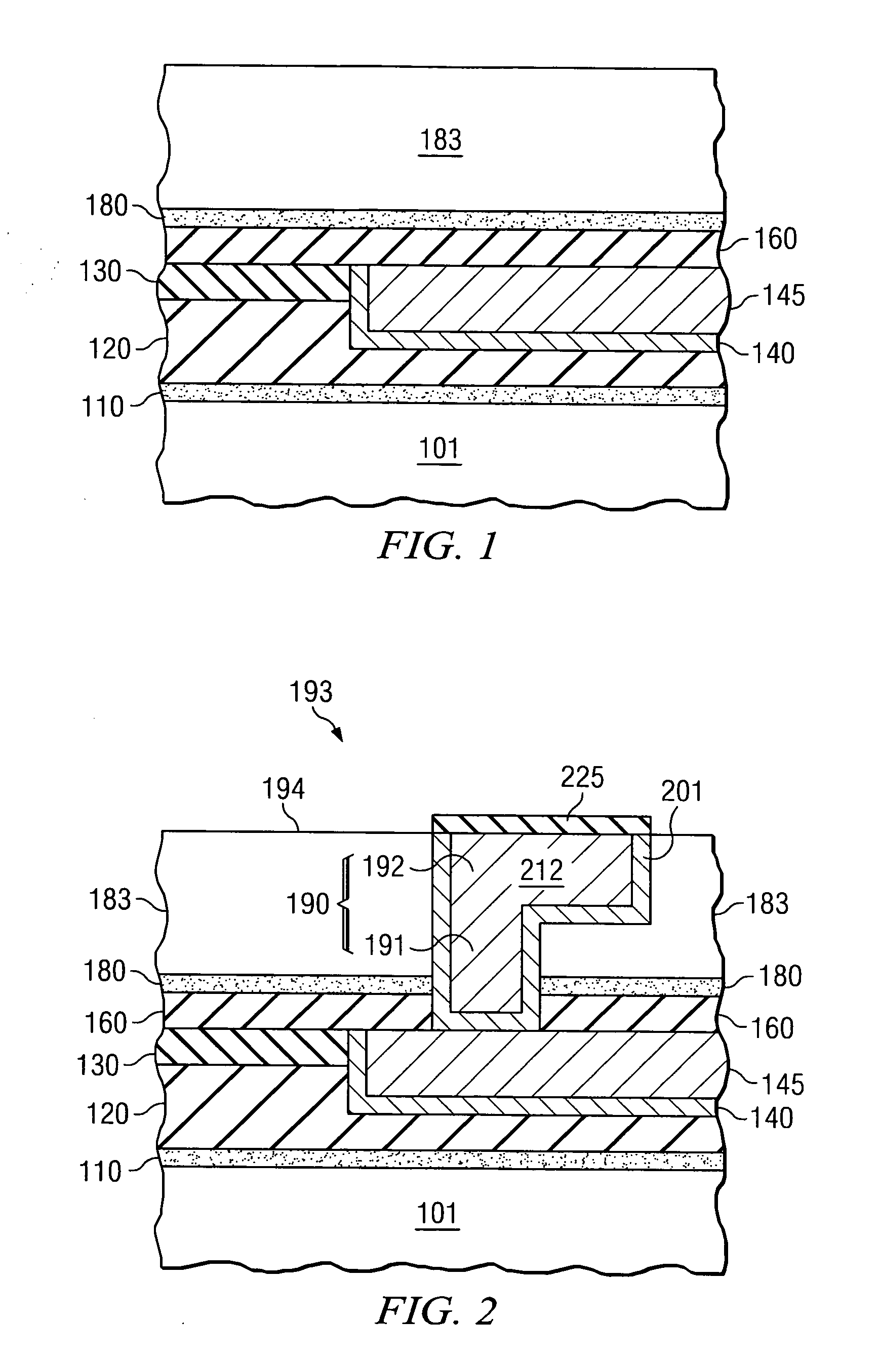
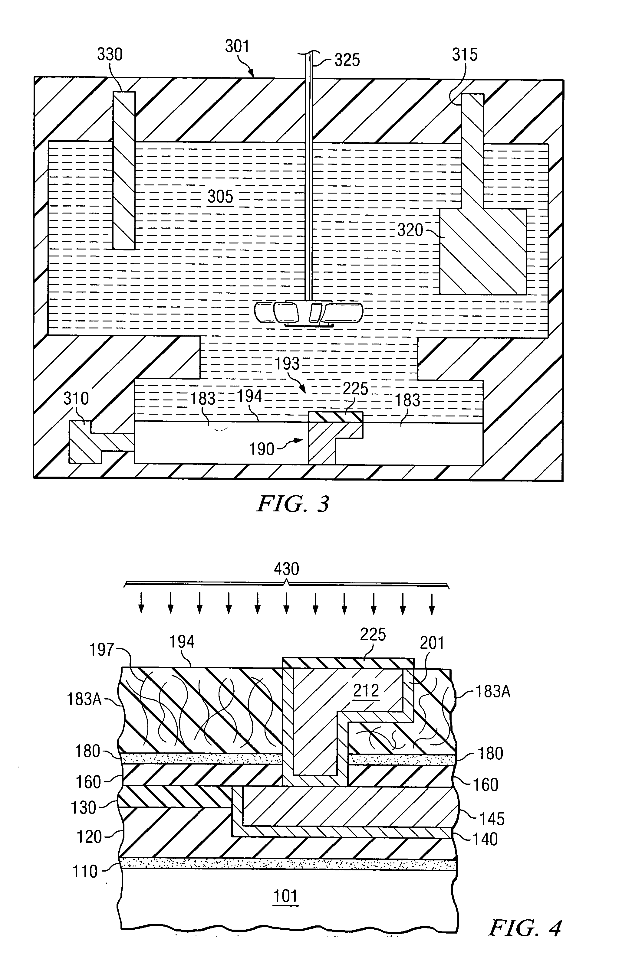
[0017] Exemplary materials, structures, and methods are provided below for fabricating a semiconductor device that has damascene interconnect structure. Although the exemplary embodiments are described as a series of steps, it will be appreciated that this is for illustration and not for the purpose of limitation. For example, some steps may occur in a different order than illustrated yet remain within the scope of the invention. Also, not all illustrated steps are necessarily required to implement the invention. Furthermore, the materials, structures, and methods according ...


PUM


Abstract

Embodiments of the invention provide a semiconductor device having dielectric material and its method of manufacture. A manufacturing method comprises forming a layer of silicon over a substrate, forming an opening through the layer of silicon, filling the opening with a conductor; and anodically etching the layer of silicon so as to form porous silicon. Embodiments may further include passivating the porous silicon such as by treating its surface with an organometallic compound. Other embodiments of the invention provide a semiconductor device comprising a layer comprising functional devices; and an interconnect structure over the layer, wherein the interconnect structure comprises a porous silicon dielectric. In an embodiment of the invention, the interconnect structure comprises a dual damascene interconnect structure. Other embodiments may include a passivation step after the step of oxidizing the porous silicon.

Description

TECHNICAL FIELD [0001] This invention relates generally to semiconductor device manufacturing and more particularly to the formation and processing of low-k dielectric films. BACKGROUND [0002] As the density of semiconductor devices increases and the size of circuit elements becomes smaller, the resistance capacitance (RC) delay time increasingly dominates the circuit performance. To reduce the RC delay, the demands on interconnect layers for connecting the semiconductor devices to each other increases. Therefore, there is a desire to switch from traditional silicon dioxide based dielectrics to low-k dielectrics. These materials are particularly useful as intermetal dielectrics, IMDs, and as interlayer dielectrics, ILDs. [0003] One example of a low-k material is fluorine-doped silicon dioxide, or fluorosilicate glass (FSG). Another widely used material is a carbon-doped oxide or organosilicate glass (OSG). OSG films typically comprise SiwCxOyHz wherein the tetravalent silicon may ha...

Claims


Application Information

Patent Timeline
IPC IPC(8): H01L21/31H01L21/469
CPCH01L21/02203H01L21/02238H01L21/02258H01L21/02304H01L21/02359H01L21/306Y10S438/958H01L21/31662H01L21/7682H01L21/76826H01L21/76832H01L21/76834H01L21/3105H01L2221/1047
Inventor WEBER, FRANK
Owner INFINEON TECH AG
Why Eureka
Try Eureka