Semiconductor physical quantity sensor of electrostatic capacitance type and method for manufacturing the same

a technology of electrostatic capacitance and semiconductors, applied in the direction of force measurement, instruments, semiconductor devices, etc., can solve the problems of inability to obtain desired sensor characteristics, inability to detect pressure, and inability to move the pressure-sensing portion b>4/b>, so as to prevent the formation of bonding voids and reduce the size of the chip

Inactive Publication Date: 2007-08-02
MATSUSHITA ELECTRIC WORKS LTD
View PDF5 Cites 6 Cited by
  • Summary
  • Abstract
  • Description
  • Claims
  • Application Information

AI Technical Summary

Benefits of technology

[0015] According to the present invention, in anodic bonding, the semiconductor substrate (movable electrode) is connected to the fixed electrode by an equipotential wiring, which is a short-circuit conductive pattern, so that the movable electrode is equipotential to the fixed electrode. This prevents discharge from occurring between both electrodes in the anodic bonding, whereby the anodic bonding is secured. This equipotential wiring is cut and removed after the end of the bonding. This electrically separates the movable electrode from the fixed electrode, making it possible to detect a physical quantity such as pressure, acceleration or the like, whereby a sensor having desired characteristics can be obtained. Furthermore, since the equipotential wiring is prevented from being sandwiched between the substrates, bonding voids are prevented from occurring. Further, since the short-circuit conductive pattern is formed on the insulating substrate inside the bonding portion, it is possible to reduce chip size.

Problems solved by technology

The occurrence of such state leads to a problem that the pressure-sensing portion 4 becomes unmovable and unable to detect a pressure.
However, with the equipotential wiring being kept formed, desired sensor characteristics cannot be obtained.
However, this short-circuit conductive pattern is formed between the glass substrate and the silicon substrate, which leads to a problem that bonding voids (condition like trapping bubbles preventing bonding) are likely to occur around the short-circuit conductive pattern.
However, in this case, a problem arises in that a chip size increases because the short-circuit conductive pattern is provided outside the bonding portion between both substrates.

Method used


Image

  • Semiconductor physical quantity sensor of electrostatic capacitance type and method for manufacturing the same
  • Semiconductor physical quantity sensor of electrostatic capacitance type and method for manufacturing the same
  • Semiconductor physical quantity sensor of electrostatic capacitance type and method for manufacturing the same

Examples


Embodiment Construction

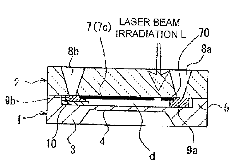
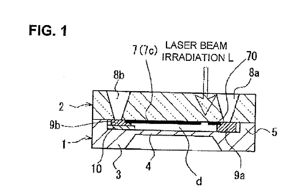
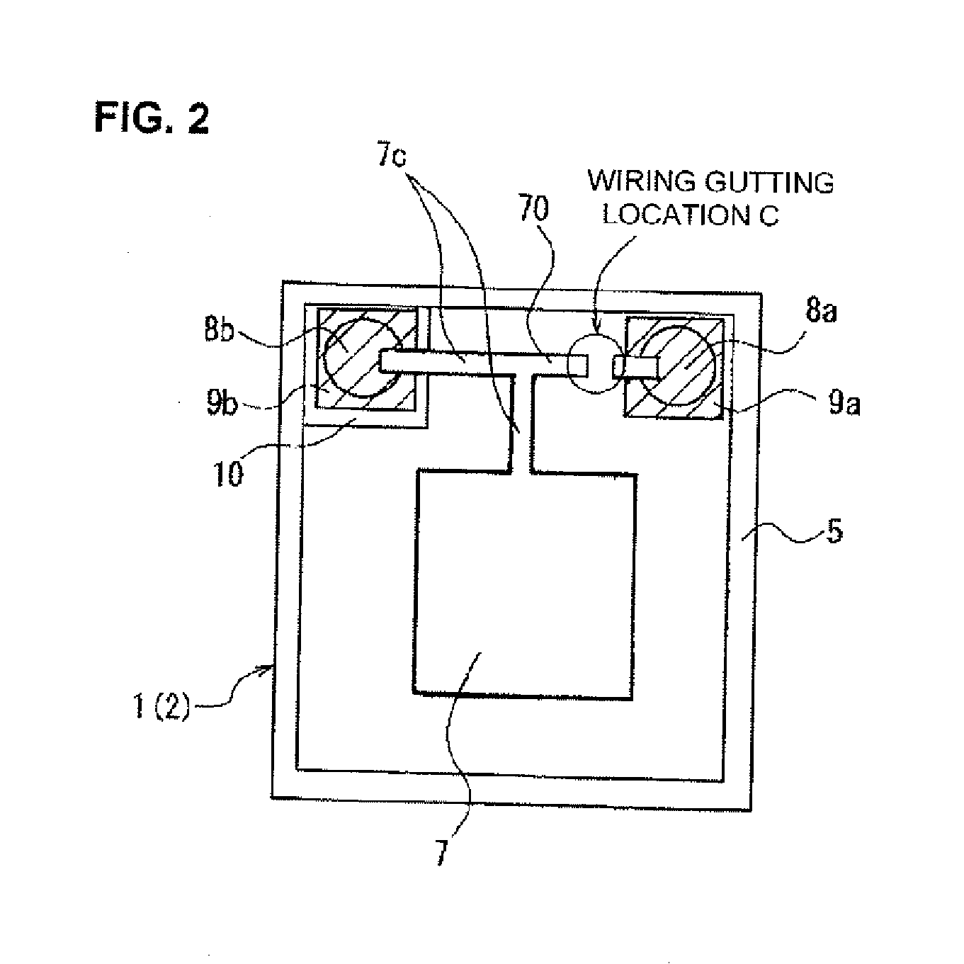
[0026] Hereinafter, a semiconductor physical quantity sensor of electrostatic capacitance type (hereafter referred to as capacitance type sensor) according to an embodiment of the present invention will be described with reference to the drawings. FIG. 1 shows a cross-sectional structure of a capacitance type sensor according to an embodiment of the present invention, while FIG. 2 is a top plan structure of the sensor, in which a glass substrate 2 is transparent, and a fixed electrode 7 and so on are shown in a see-through manner. The drawings show a silicon substrate 1 (semiconductor substrate) as a wafer corresponding to one sensor chip part together with the glass substrate 2 (insulating substrate), while in an actual manufacturing process, areas corresponding to the glass substrate 2 are allocated on the surface of a large glass substrate. This similarly applies to the silicon substrate 1.

[0027] Before anodic bonding to bond both substrates, the fixed electrode 7 and lead porti...


PUM


Abstract

In a semiconductor physical quantity sensor of electrostatic capacitance type, mutually facing peripheral areas (bonding areas) of a glass substrate and a silicon substrate are contacted for anodic bonding, while at the same time, both substrates have an anodic bonding voltage applied therebetween so as to be integrated. A fixed electrode is formed on a bonding face-side surface of the silicon substrate, while a movable electrode is formed on a bonding face-side surface of the semiconductor substrate. An equipotential wiring, which short-circuits the fixed electrode to the movable electrode as a countermeasure to discharge in anodic bonding, is formed on the bonding face-side surface of the glass substrate inside the bonding area before the anodic bonding. After the anodic bonding, the equipotential wiring is cut and removed. By manufacturing the sensor in this manner, the fixed electrode of the insulating substrate is made equipotential to the movable electrode of the semiconductor substrate when the insulating substrate is anodically bonded to the semiconductor substrate, thereby preventing discharge from occurring. Accordingly, it is possible to obtain a high bonding strength and desired sensor characteristics without causing bonding voids to occur and a sensor chip to increase in size.

Description

TECHNICAL FIELD [0001] The present invention relates to a semiconductor physical quantity sensor of electrostatic capacitance type as a MEMS (Micro Electro Mechanical System) device and a method for manufacturing the same, and more particularly to a countermeasure to discharge in anodic bonding. BACKGROUND ART [0002] An example of a conventional semiconductor physical quantity sensor of electrostatic capacitance type is shown in FIG. 8. As shown therein, an insulating glass substrate 2 is placed on an upper surface of a silicon semiconductor substrate 1 (hereafter referred to as silicon substrate), in which both substrates 1, 2 are bonded at peripheral areas thereof (joining areas) 5 by anodic bonding. The silicon substrate 1 is etched to form a frame-shaped support mounting 3 having a pressure-sensing portion 4 thin-walled relative thereto to be flexible and movable up and down. Each of the upper and lower surfaces of the pressure-sensing portion 4 serves as a movable electrode, wh...

Claims


Application Information

Patent Timeline
Patent Type & Authority Applications(United States)
IPC IPC(8): H01L29/84H01L21/00
CPCG01L9/0042G01L1/14H01L29/84
Inventor MESHII, RYOSUKESAKAI, KOUJIISHIGAMI, ATSUSHIFURUKUBO, EICHI
Owner MATSUSHITA ELECTRIC WORKS LTD
Why Eureka
Try Eureka