Image display device

a technology of image display device and driver circuit, which is applied in the direction of instruments, static indicating devices, etc., can solve the problems of high power consumption of data lines and the data driver circuit for driving the data lines, and achieve the effect of reducing power consumption, reducing power consumption, and reducing power consumption

Active Publication Date: 2007-08-02
PANASONIC LIQUID CRYSTAL DISPLAY CO LTD +1
View PDF2 Cites 26 Cited by
  • Summary
  • Abstract
  • Description
  • Claims
  • Application Information

AI Technical Summary

Benefits of technology

[0026]According to the aspect of the invention, it is possible to reduce power consumption required to rewrite pixel circuits and therefore lower the power consumption of an image display device. Particularly in an image display device, such as a reflective liquid crystal display device or a semi-transmissive liquid crystal display device, in which mos

Problems solved by technology

Thus, in either case of displaying a moving image or a static image, data lines for transferring data signals to pixels needs to be

Method used


Image

  • Image display device
  • Image display device
  • Image display device

Examples


Embodiment Construction

[0043]Preferred embodiments of an image display device according to the present invention will be described with reference to the accompanying drawings.

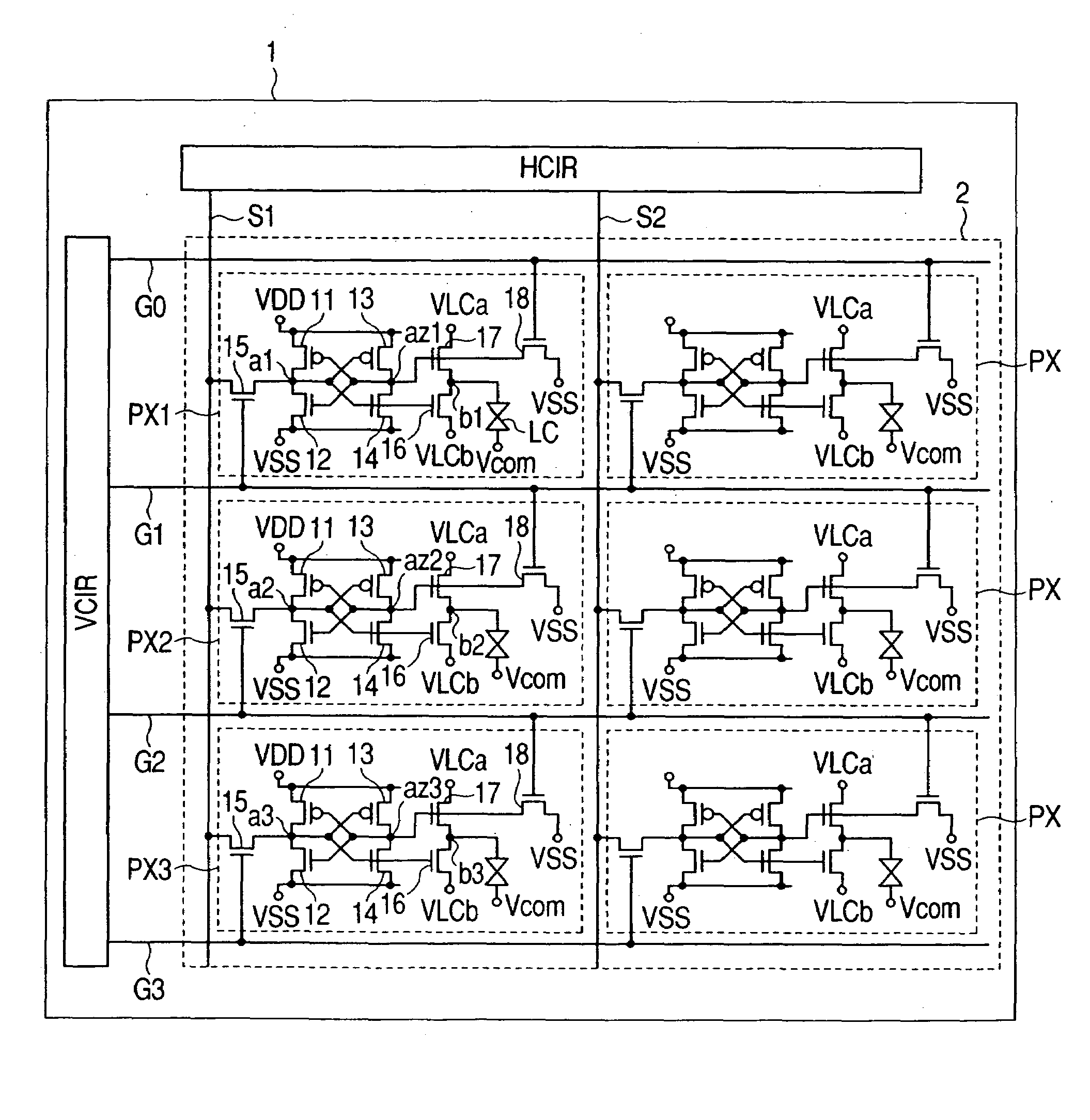
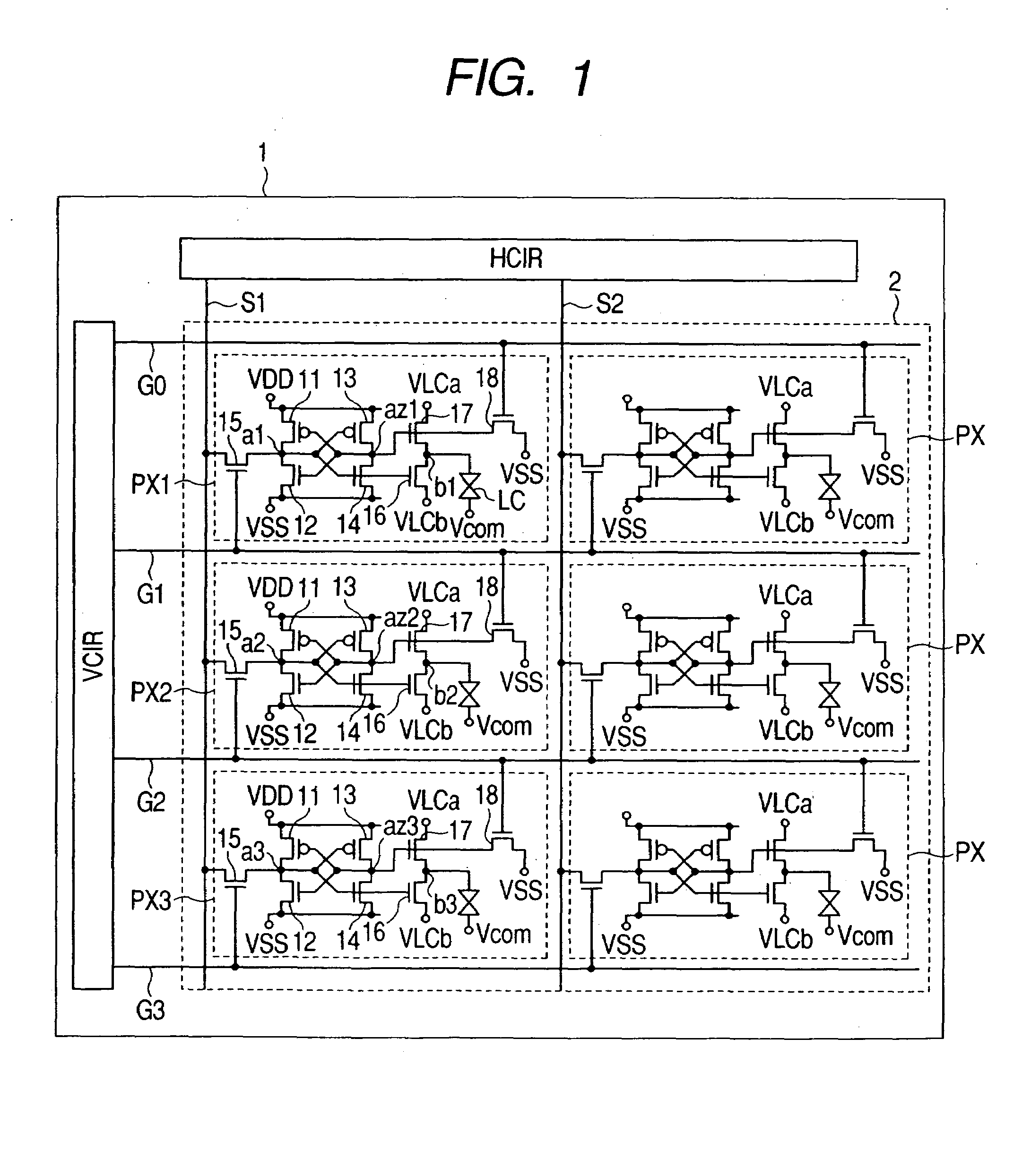
[0044]FIG. 1 shows the circuit configuration of the image display device according to the invention. There are formed over a glass substrate 1 a data driver circuit HCIR, a scanning circuit VCIR, and a display area 2. The glass substrate 1 is a substrate that is generally used in a low-temperature polysilicon manufacturing process. However, the material of the substrate is not limited to glass as long as insulation on the surface is secured. On the display area 2, a plurality of data lines S1 to S2 are wired in vertical directions and a plurality of gate lines G0 to G3 are wired in horizontal directions. Pixel circuits PX and PX1 to PX3 are disposed at intersections. The pixel circuits PX1 to PX3 are the same as the pixel circuits PX; however, they are indicated as PX1 to PX3 for identification in later description.

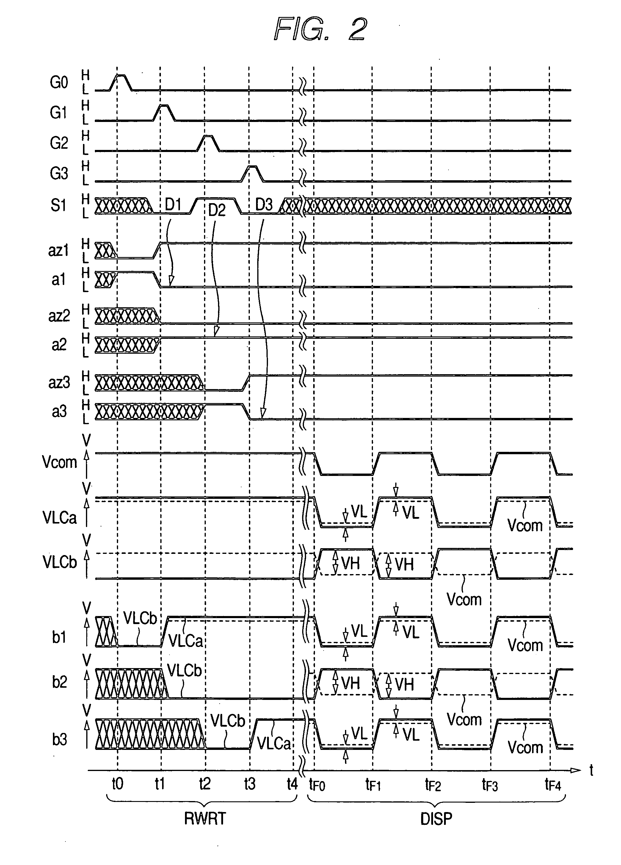
[0045]In FIG. 1, t...


PUM


Abstract

The present invention provides an image display device having about the same numbers of gate lines and data lines as before and capable of reducing the power consumption of a static memory during rewriting of a display image. In the configuration of the image display device, the drain electrode of a first transistor 15 included in a pixel circuit is connected to an input for setting a storing state of the static memory, the drain electrode of a second transistor 18 is connected to an input for resetting a storing state of the static memory, the source electrode of the first transistor is connected to a data line, the gate electrode of the first transistor included in a row of pixel circuits arranged parallel to gate lines is connected to one gate line of the plurality of gate lines, and the gate electrode of the second transistor included in another row of pixel circuits arranged adjacent to the row of pixel circuits is connected to the one gate line.

Description

CLAIM OF PRIORITY[0001]The present application claims priority from Japanese application JP 2006-018500 filed on Jan. 27, 2006, the content of which is hereby incorporated by reference into this application.FIELD OF THE INVENTION[0002]The present invention relates to an image display device and a driver circuit thereof, and more particularly to an image display device incorporating a static memory in each pixel circuit and having reduced power consumption.BACKGROUND OF THE INVENTION[0003]In an active matrix type display, typically an active matrix type liquid crystal display, a thin film transistor (hereinafter abbreviated as TFT) is formed in each pixel, and display information is stored on a pixel-by-pixel basis to display images. A TFT formed by using a polysilicon film which is fabricated by polycrystallization of an amorphous silicon film by laser annealing, with its mobility being raised to about 100 cm2 / VS is called a polysilicon TFT. Since a circuit configured of such polysi...

Claims


Application Information

Patent Timeline
IPC IPC(8): G09G3/36
CPCG09G3/3659G09G2300/0809G09G2330/021G09G2310/0251G09G2300/0857
Inventor KAGEYAMA, HIROSHIMATSUMOTO, KATSUMIMIYAZAWA, TOSHIO
Owner PANASONIC LIQUID CRYSTAL DISPLAY CO LTD
Why Eureka
Try Eureka