Methods of preventing defects in antireflective coatings

a technology of anti-reflective coating and coating layer, applied in the field of new, can solve the problems of non-uniform photoresist linewidth upon development, non-uniform photoresist linewidth, and difficulty in achieving the effect of accelerating the development of pinhole defects

Inactive Publication Date: 2007-08-02
IBM CORP
View PDF11 Cites 12 Cited by
  • Summary
  • Abstract
  • Description
  • Claims
  • Application Information

AI Technical Summary

Benefits of technology

[0017]The present invention relates to a method that that uses a vacuum step at a reduced ambient temperature to strip the solvent from the resist film. The polymer can then be cross-linked at or near ambient temperature, avoiding the high temperature heating cycle that can accelerate the development of pinhole defects.

Problems solved by technology

Reflection of the activating radiation used to expose a photoresist often poses notable limits on resolution of the image patterned in the resist layer.
Reflection of radiation from the substrate / resist interface can produce variations in the radiation intensity in the resist during exposure, resulting in non-uniform photoresist linewidth upon development.
The amount of scattering and reflection will typically vary from region to region, resulting in further linewidth non-uniformity.
Due to radiation reflection at the resist / substrate interface, however, constructive and destructive interference is particularly significant when monochromatic or quasi-monochromatic radiation is used for photoresist exposure.
In such cases, the reflected light interferes with the incident light to form standing waves within the resist.
In the case of highly reflective substrate regions, the problem is exacerbated since large amplitude standing waves create thin layers of underexposed resist at the wave minima.
The underexposed layers can prevent complete resist development causing edge acuity problems in the resist profile.
If the resist thickness is non-uniform, the problem becomes more severe, resulting in variable linewidth control.
Variations in substrate topography also give rise to resolution-limiting reflection problems.
Any image on a substrate can cause impinging radiation to scatter or reflect in various uncontrolled directions, affecting the uniformity of resist development.
As substrate topography becomes more complex with efforts to design more complex circuits, the effects of reflected radiation become more critical.
For example, metal interconnects used on many microelectronic substrates are particularly problematic due to their topography and regions of high reflectivity.
Some workers have found that use of such dyes can limit resolution of the patterned resist image.
At least some prior antireflective coatings, however, suffer from poor adhesion to the overcoated photoresist layer and / or the underlying substrate surface.
Such adhesion problems can severely compromise the resolution of the patterned photoresist image.
Thin ARC films have been shown to have a tendency to spontaneously dewet during the post-apply-bake step, creating pinhole defects.
This problem becomes more and more common as films move to thinner thickness ranges associated with next-generation lithographic nodes.
Currently, there are no good techniques to solve this problem aside from using thicker ARCs which are less prone to destabilization.
This particular problem places an additional burden on the lithography method.
In addition, once the film temperature approaches the bake plate temperature, a thermally activated crosslinking agent “freezes” the film at which point it is stabilized and pinhole defects can no longer develop.
While this methodology has worked well for many generations of semiconductor manufacturing, it becomes problematic as the technology approaches ultra-thin spin-cast organic films.
As films become this thin, the potential for spontaneous dewetting is enhanced in a very non-linear fashion, leading to pinhole defects throughout the BARC film.

Method used


Image

  • Methods of preventing defects in antireflective coatings
  • Methods of preventing defects in antireflective coatings

Examples


example 1

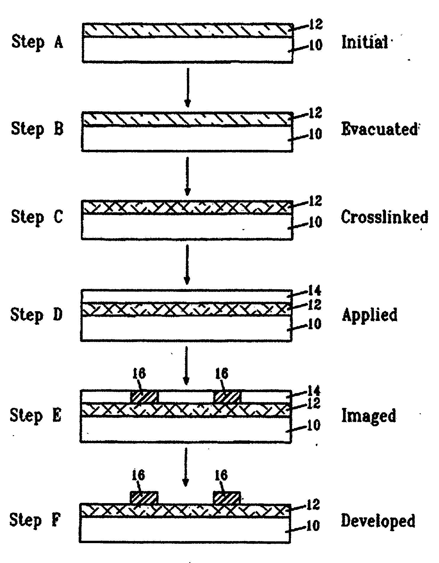
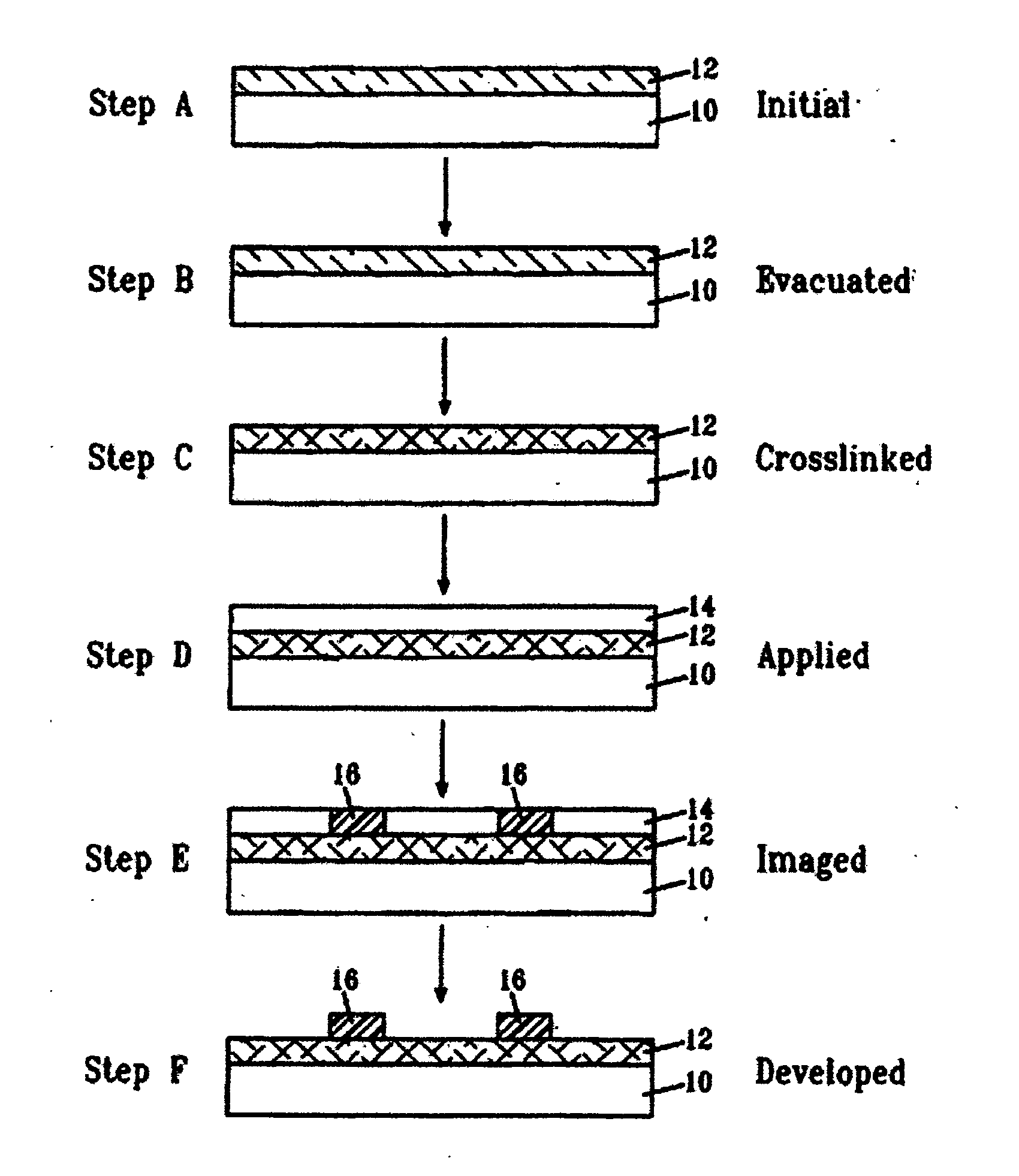
[0106]Two bare silicon wafers with a thin native oxide coating were coated with an ARC on a lithography track. The wafers were then subjected to a mild vacuum-strong vacuum to remove residual solvent. By “mild vacuum”, it is meant 10−5 Torr. By “strong vacuum”, it is meant 10−7 Torr. The wafers were then returned to the lithography track and baked at conventional bake temperature.

[0107]The total number of pinhole defects in each of the two wafers were 9 and 5 in the mild vacuum and 5 and 5 in the strong vacuum (See Table 1). These results show that there was a significant reduction in the total number of defect counts on the wafers that had intermediate and strong vacuum based solvent strip compared to the wafers without a vacuum based solvent strip.

[0108]Following this vacuum exposure step, the substrate was placed on a hotplate to activate the crosslinking agent. Commercially available AR40 BARC, was baked at a conventional 215° C. bake temperature for 60 seconds. Results are show...


PUM

PropertyMeasurementUnit
temperatureaaaaaaaaaa

Abstract

A method of forming a relief image on a substrate including: applying over a substrate a layer of an antireflective coating; and vacuum processing the antireflective coating. This method reduces the number of pinhole defects present in the antireflective coating.

Description

BACKGROUND OF THE INVENTION[0001]1. Field of the Invention[0002]The present invention relates to new methods of making antireflective coatings. More particularly, the present invention relates to new methods of reducing defects in antireflective coatings.[0003]2. Background Art[0004]Photoresists are used for transfer of an image to a substrate. A coating layer of a photoresist is formed on a substrate, and the resist layer is then selectively exposed through a photomask to a source of activating radiation. The photomask has areas that are opaque to activating radiation and other areas that are transparent to activating radiation. Exposure to activating radiation provides a photoinduced chemical transformation of the photoresist coating to thereby transfer the pattern of the photomask to the resist coated substrate. Following exposure, the photoresist is developed to provide a relief image that permits selective patterning of the substrate.[0005]A photoresist can be either positive-a...

Claims


Application Information

Patent Timeline
Patent Type & Authority Applications(United States)
IPC IPC(8): G03C1/00
CPCG03F7/091
Inventor BRODSKY, COLIN J.BRODSKY, MARY JANELI, WAI-KINSCHEER, STEVEN A.
Owner IBM CORP
Why Eureka
Try Eureka