Simplified power-down mode control circuit utilizing active mode operation control signals
- Summary
- Abstract
- Description
- Claims
- Application Information
AI Technical Summary
Benefits of technology
Problems solved by technology
Method used
Image


Examples
Embodiment Construction
[0054] Reference will now be made in greater detail to a preferred embodiment of the invention, an example of which is illustrated in the accompanying drawings. Wherever possible, the same reference numerals will be used throughout the drawings and the description to refer to the same or like parts.
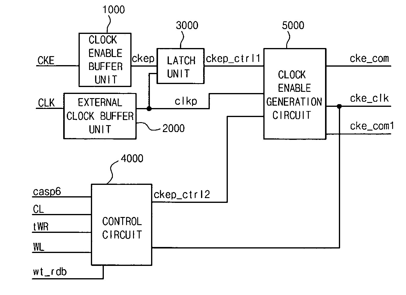
[0055]FIG. 6 is a circuit block diagram for illustrating a circuit for entering into a power-down mode in a semiconductor memory device in accordance with an embodiment of the present invention.
[0056] Referring to FIG. 6, a semiconductor memory device according to an embodiment of the present invention includes, inter alia:
[0057] (1) a clock enable buffer unit 1000 that receives an external clock enable signal CKE when entering a power-down mode and outputs the inputted CKE signal as a buffered clock enable pulse signal ckep;
[0058] (2) an external clock buffer unit 2000 that receives an external clock signal CLK and outputs the inputted CLK signal as a buffered external clock pulse si...
PUM
 Abstract
Description
Claims
Application Information
 - R&D
- Intellectual Property
- Life Sciences
- Materials
- Tech Scout
- Unparalleled Data Quality
- Higher Quality Content
- 60% Fewer Hallucinations
Browse by: Latest US Patents, China's latest patents, Technical Efficacy Thesaurus, Application Domain, Technology Topic, Popular Technical Reports.
© 2025 PatSnap. All rights reserved.Legal|Privacy policy|Modern Slavery Act Transparency Statement|Sitemap|About US| Contact US: help@patsnap.com