Systems, Masks, and Methods for Photolithography

Active Publication Date: 2007-08-09
KLA TENCOR TECH CORP
View PDF99 Cites 60 Cited by
  • Summary
  • Abstract
  • Description
  • Claims
  • Application Information

AI Technical Summary

Benefits of technology

[0014] Aspects may provide for blocks to be processed using any of the methods described above. In some embodiments, blocks may be processed in parallel using multiple processors, blades or accelerator cards. Aspect

Problems solved by technology

However, due to the wave nature of light, as dimensions approach sizes comparable to the wavelength of the light used in the photolithography process, the resulting wafer patterns deviate from the corresponding photomask patterns and are accompanied by

Method used


Image

  • Systems, Masks, and Methods for Photolithography
  • Systems, Masks, and Methods for Photolithography
  • Systems, Masks, and Methods for Photolithography

Examples


example masks

and Integrated Circuits

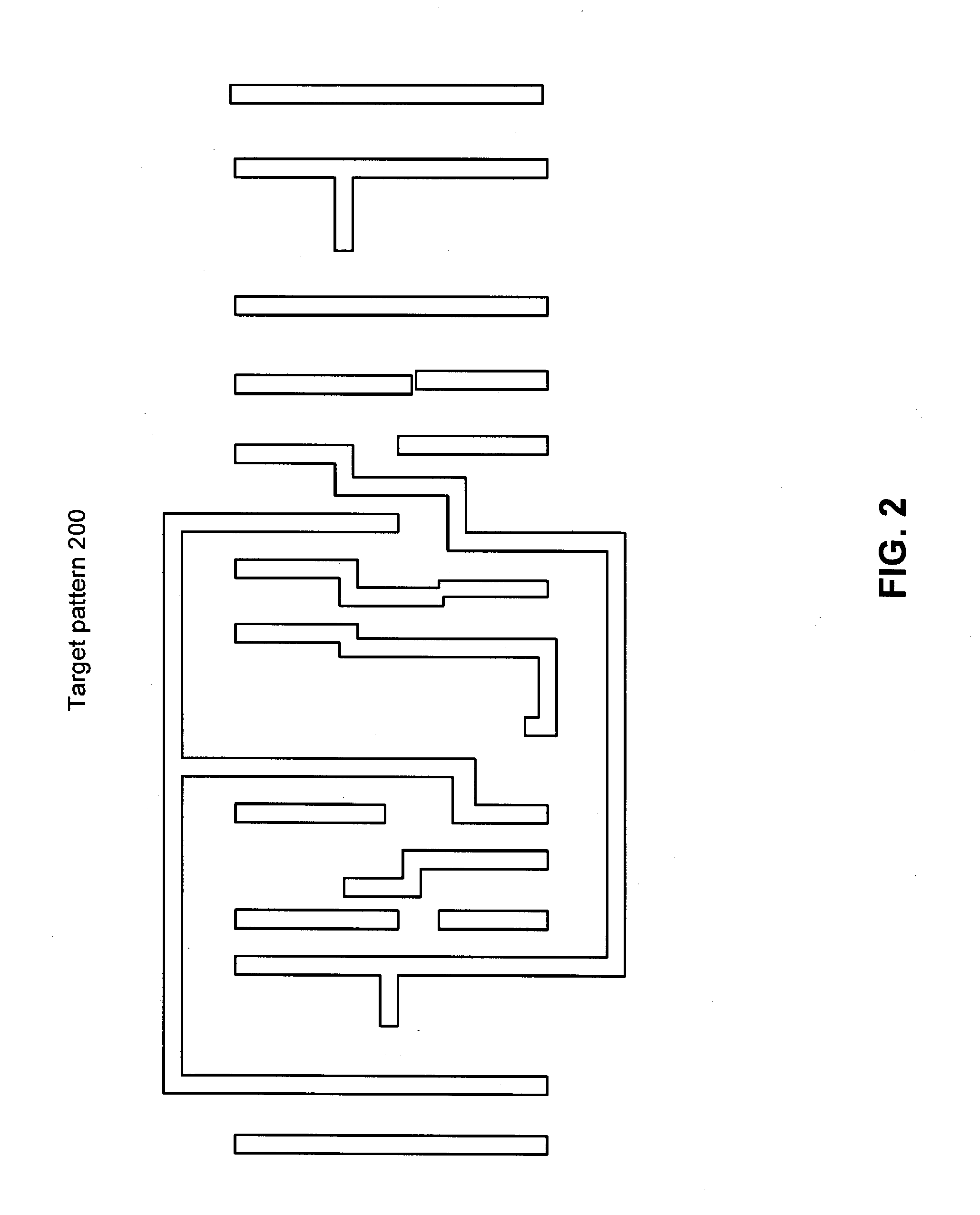
[0182] Photomasks may be manufactured using the mask pattern generated by the above systems and methods. Chrome, clear or phase shifted regions may be formed on a photomask in accordance with the mask pattern. For instance, FIGS. 15, 16, 17, 18B, C and D, 19B, C, D, E and F and 20B, C, D and E illustrate sample patterns that result from systems and methods according to example embodiments of the present invention. In these figures, the example patterns correspond to individual blocks of an overall photomask, although it will be understood that blocks may be combined into an overall pattern to be used in manufacturing a photomask.

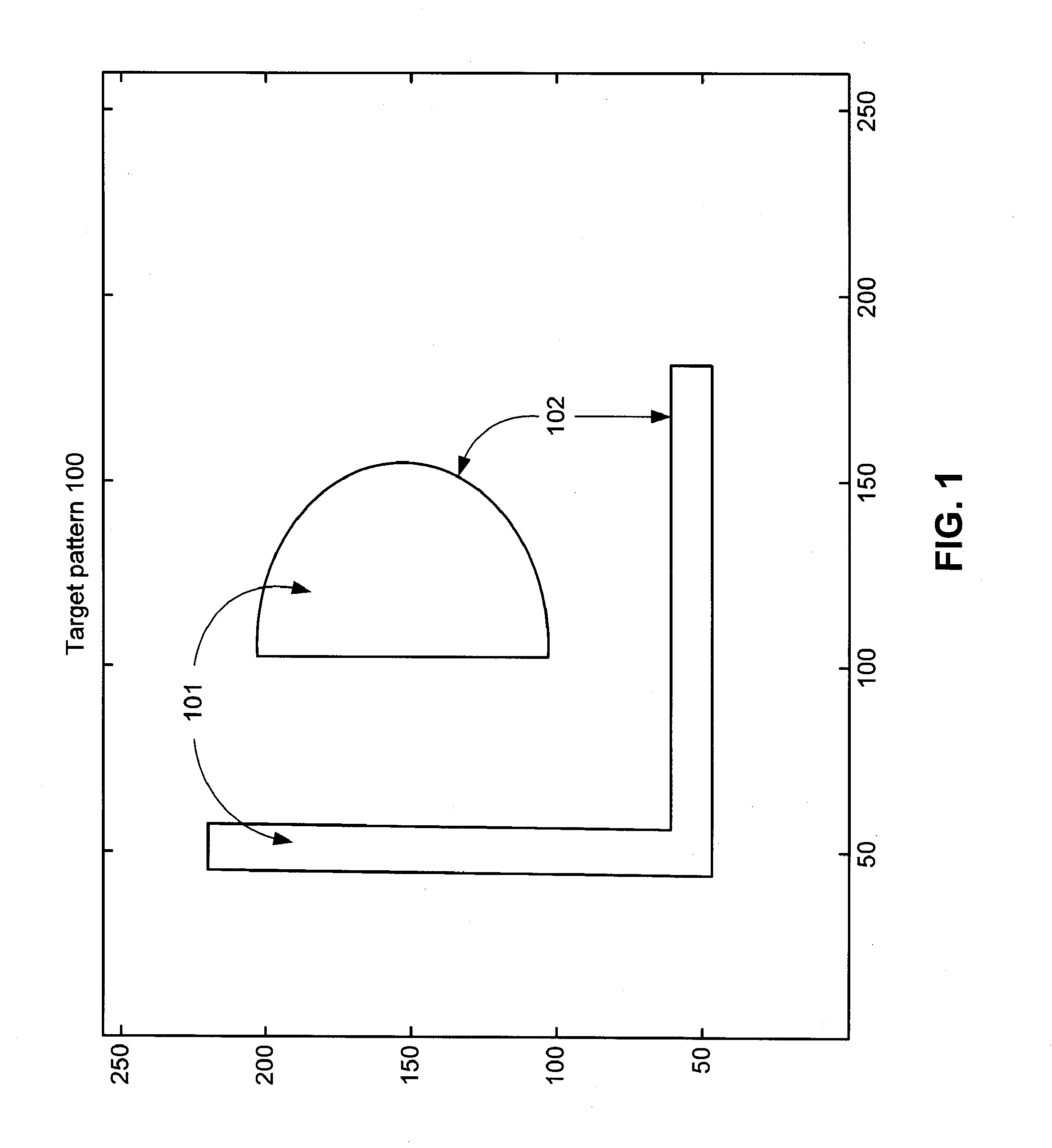
[0183]FIG. 15 shows an example pattern for block 1500. This block is about one micron square. This block has a target pattern 1502 that is an isolated rectangle of 100 nm×454 nm. The process parameters (provided as inputs) include an illumination wavelength of 193 nm, a numerical aperture of 0.85, a point source of illumination, an at...


PUM


Abstract

Photomask patterns are represented using contours defined by mask functions. Given target pattern, contours are optimized such that defined photomask, when used in photolithographic process, prints wafer pattern faithful to target pattern. Optimization utilizes “merit function” for encoding aspects of photolithographic process, preferences relating to resulting pattern (e.g. restriction to rectilinear patterns), robustness against process variations, as well as restrictions imposed relating to practical and economic manufacturability of photomasks.

Description

CROSS-REFERENCE [0001] This application claims the benefit of U.S. Provisional Application No. 60 / 775,991, filed Sep. 13, 2005, which is incorporated herein by reference in its entirety.BACKGROUND OF THE INVENTION [0002] 1. Field of Invention [0003] Field relates to masks, also known as photomasks, used in photolithography processes and, more particularly, to a method for finding the optimal photomask pattern to allow for production of wafer patterns with minimal distortions or artifacts and to allow for the ability to constrain resulting contours to rectilinear patterns. [0004] 2. Description of Related Art [0005] Lithography processing represents an essential technology for manufacturing Integrated Circuits (IC) and Micro Electro-Mechanical Systems (MEMS). Lithographic techniques are used to define patterns, geometries, features, shapes, et al (“patterns”) onto an integrated circuit die or semiconductor wafer or chips where the patterns are typically defined by a set of contours, ...

Claims


Application Information

Patent Timeline
IPC IPC(8): G06F17/50G03F1/00
CPCG03F1/36G03F1/144G03F1/70G03F1/72G03F7/70491
Inventor ABRAMS, DANIEL S.OSHER, STANLEYPENG, DANPING
Owner KLA TENCOR TECH CORP
Why Eureka
Try Eureka