Pasting method and pasting apparatus

a technology which is applied in the field of paste method and paste apparatus, can solve the problems of increasing size, warping and cracking of semiconductor wafers, and becoming an unignorable problem, and achieve the effects of not easily displaced, thin plate, and separation from the member in a very short tim

Inactive Publication Date: 2007-08-16
TOKYO ELECTRON LTD
View PDF9 Cites 3 Cited by
  • Summary
  • Abstract
  • Description
  • Claims
  • Application Information

AI Technical Summary

Benefits of technology

[0015] The present invention uses the liquid crystal wax for pasting together the thin plate and the member. The liquid crystal wax changes its phase between a liquid phase and a solid phase at a predetermined temperature. Therefore, the thin plate can be pasted to the member and can be separated from the member in a very short time and hence the thin plate is not displaced easily.
[0016] According to the first to the fourth aspect of the present invention, the thin plate and the member are held vertically opposite to each other with their joining surfaces extended in high flatness so as to be moved in directions along an X-axis, a Y-axis and a Z-axis and to be turned in a θ-direction relative to each other. Therefore, the joining surfaces extended in satisfactory flatness can be accurately joined together. Since the liquid-phase liquid crystal wax held between the thin plate and the member is spread in a liquid-phase liquid crystal wax layer over the surfaces of the thin plate and the member by moving the thin plate and the member relative to each other, the liquid-phase liquid crystal wax layer will not contain bubbles and the thin plate and the member can be surely pasted together with the liquid crystal wax layer of a uniform thickness.
[0017] According to the second and the fourth aspect of the present invention, the respective positions of the thin plate and the member are recognized and the thin plate and the member are aligned with each other on the basis of the information about the positions of the thin plate and the member. Thus the thin plate and the member can be further accurately pasted together. More concretely, the thin plate and the member can be very accurately pasted together by positioning the thin plate and the member in a plane and adjusting the parallelism between the thin plate and the member.
[0018] According to the fifth and the sixth aspect of the present invention, the two thin metal plates are supplied individually and continuously, the two thin metal plates are guided for downward movement with the two thin metal plates spaced from each other by a space of a predetermined thickness, the liquid crystal was is poured into the space between the two thin metal plates, and the two thin metal plates holding the liquid crystal wax and moving downward are pressed to paste the two thin metal plates together. Thus the two thin metal plates can be surely and accurately pasted together without developing any bubbles in the liquid crystal wax.

Problems solved by technology

Warping and cracking of semiconductor wafers (hereinafter, referred to simply as “wafers”) have become an unignorable problem with the progressive increase in size of wafers and the progressive decrease in thickness of wafers in semiconductor device fabricating processes.
If a wafer held by an electrostatic chuck warps, for example, during a wafer carrying process, a chemical-mechanical polishing process (COM process), a dry etching process or an ion-implantation process, the wafer cannot be accurately processed or is liable to crack.
When wax is used for pasting a wafer to a backing substrate, it takes a comparatively long time for the liquid-phase liquid crystal wax to solidify into the solid-phase wax.
Thus, processes for pasting the wafer to the backing substrate and for separating the wafer from the backing substrate need a long time.
The wafer is liable to be displaced before the wax solidifies because the wax takes a long time to solidify.
It is difficult to spread the wax not containing bubbles in a uniform thickness over a surface of the wafer and to paste the wafer accurately in a satisfactory flatness to the backing substrate by using only the stamper or the gage block.
When the technique disclosed in JP 8-139165 A or JP 10-12578 A is used in combination with the multilayer packaging technique, a problem arises in processing time and accuracy and it is difficult for those previously proposed techniques to paste a foil having a thickness not greater than 100 μm to the backing substrate.

Method used


Image

  • Pasting method and pasting apparatus
  • Pasting method and pasting apparatus
  • Pasting method and pasting apparatus

Examples


first embodiment

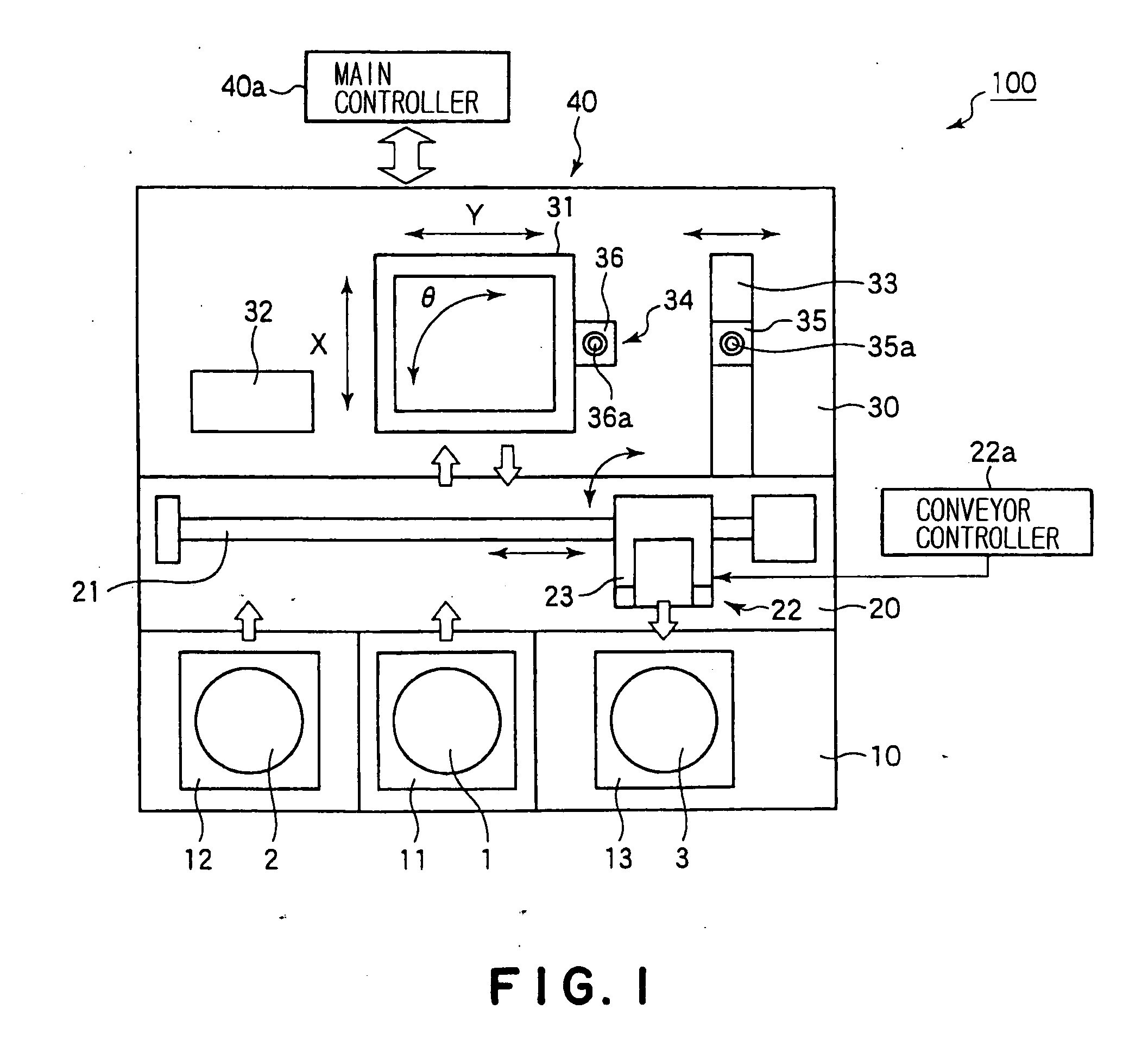
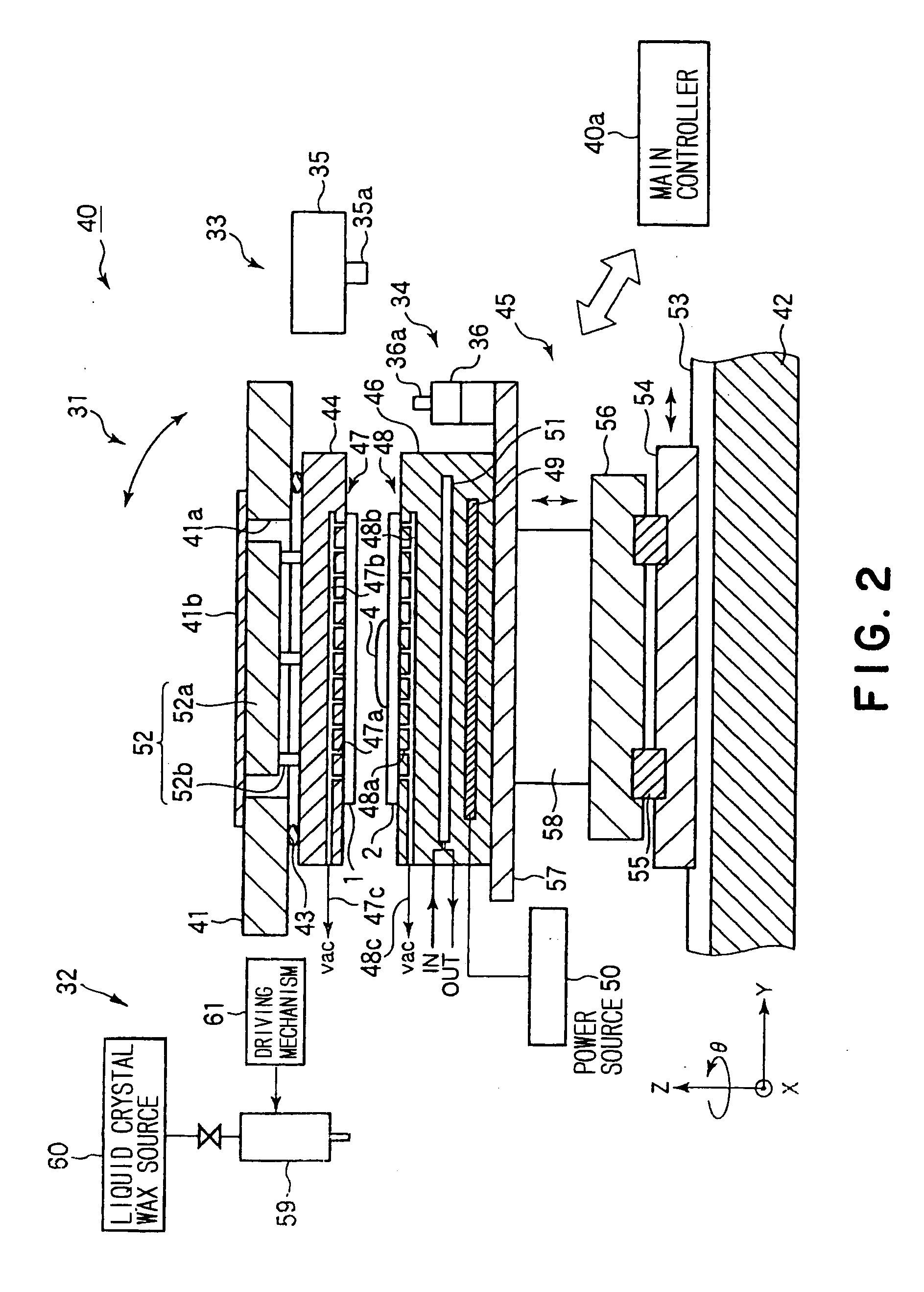
[0031] The pasting unit 30 is provided with a pasting apparatus 40 in a first embodiment according to the present invention. The pasting apparatus 40 includes a main unit 31 disposed in a central part thereof, and a liquid crystal wax pouring mechanism 32 disposed beside the main unit 31. The liquid crystal wax pouring mechanism 32 pours a liquid crystal wax onto the carrying member 2 being carried. The pasting apparatus 40 has an upper position recognizing mechanism 33 and a lower position recognizing mechanism 34. A main controller 40a controls the pasting apparatus 40.

[0032] The loading and unloading unit 10 is provided with a thin plate cassette 11 for holding thin plates 1 therein, a carrying member cassette 12 for holding carrying members 2, and an end product cassette 13 for holding end products 3 each formed by pasting the thin plate 1 and the carrying member 2 together. The thin plate 1 is, for example, a silicon wafer or a metal foil, such as a copper foil.

[0033] The carr...

second embodiment

[0065] A pasting apparatus 80 in a second embodiment according to the present invention will be described.

[0066] Referring to FIG. 9 showing the pasting apparatus 80 in the second embodiment in a sectional view, the pasting apparatus 80 pastes together a metal foil 81, such as a copper foil, and a metal carrying member 82 made of a metal, such as a stainless steel. A first roll 91 for supplying the metal foil 81 and a second roll 92 for supplying the metal carrying member 82 are disposed parallel to each other. The metal foil 81 supplied from the first roll 91 and the. metal carrying member 82 supplied from the second roll 92 are guided obliquely downward so as to approach each other.

[0067] The metal foil 81 and the metal carrying member 82 are guided by guide rollers 93 so as to run downward with a space formed between the metal foil 81 and the metal carrying member 82. A dispenser 94 is disposed above the guide rollers 93 to pour a liquid crystal wax into the space between the me...


PUM

PropertyMeasurementUnit
thicknessaaaaaaaaaa
thicknessaaaaaaaaaa
thicknessaaaaaaaaaa

Abstract

A pasting method and a pasting apparatus hold a thin plate 1 and a planar member 2 in high flatness respectively on a first holding member 44 and a second holding member 44, a main controller 40a controls a moving mechanism 45 and a parallelism adjusting mechanism 52 on the basis of information provided by position recognizing mechanisms 33 and 34 to align the thin plate 1 and the carrying member 2 with each other in a predetermined positional relation. The main controller 40a controls a moving mechanism 45 so as to move the thin plate 1 and the carrying member 2 relative to each other in a state where a liquid-phase liquid crystal wax heated by a heater 49 is held between the thin plate 1 and the carrying member 2 to spread the liquid-phase liquid crystal wax over the entire surfaces of the thin plate 1 and the carrying member 2. Thus the thin plate 1, such as a semiconductor wafer or a metal foil, can be accurately, surely and efficiently pasted to the carrying member 2, and the thin plate 1 pasted to the carrying member 2 can be readily separated from the carrying member 2.

Description

TECHNICAL FIELD [0001] The present invention relates to a pasting method of pasting a thin, flat object, such as a semiconductor wafer or a metal foil, to another object, and a pasting apparatus for carrying out the pasting method. BACKGROUND ART [0002] Warping and cracking of semiconductor wafers (hereinafter, referred to simply as “wafers”) have become an unignorable problem with the progressive increase in size of wafers and the progressive decrease in thickness of wafers in semiconductor device fabricating processes. If a wafer held by an electrostatic chuck warps, for example, during a wafer carrying process, a chemical-mechanical polishing process (COM process), a dry etching process or an ion-implantation process, the wafer cannot be accurately processed or is liable to crack. [0003] To avoid such a trouble, a previously proposed technique subjects a wafer pasted to a backing substrate with an adhesive, such as wax, to a polishing process or the like. For example, a technique...

Claims


Application Information

Patent Timeline
Patent Type & Authority Applications(United States)
IPC IPC(8): B29C39/10B32B37/12B32B38/18H01L21/68H01L21/00H01L21/304H01L21/683
CPCB32B37/1284B32B38/1833H01L27/14634H01L21/67092B32B2038/1891H01L21/68H01L21/02
Inventor ARUGA, TSUYOSHIHAGIHARA, JUNICHIOKASE, WATARUYAMAGUCHI, EIJI
Owner TOKYO ELECTRON LTD
Why Eureka
Try Eureka