Waveguide photodetector

a waveguide and photodetector technology, applied in the field of optical waveguides, can solve the problems of limiting the development of highly scalable soi interconnects to date, unable to effectively detect such applications, and limiting the operational wavelength range of light propagation

Active Publication Date: 2007-08-16
IBM CORP
View PDF12 Cites 59 Cited by
  • Summary
  • Abstract
  • Description
  • Claims
  • Application Information

AI Technical Summary

Problems solved by technology

The lack of an effective photodetector for such applications has, however, impeded the development of highly scalable SOI interconnects to date.
However, if the waveguides of the interconnect system are made of Si, the operational wavelength range for light propagation is restricted to approximately 1.1 to 1.8 microns, where Si is transparent.
Typical Ge detectors, however, are vertically incident and thus are not compatible with monolithically integrated photonics on a SOI substrate.
Horizontal in-plane implementation is also made difficult due to the large differences in relative refractive index between Si (approximately 3.5) and Ge (approximately 4.2), which complicates efficient coupling of light from the waveguide to the photodetector.
Typical Ge detectors are also multimoded, which prevents efficient coupling between the waveguide and the photodetector.
Moreover, typical Ge detectors in general suffer from large dark current and impaired bandwidth.

Method used


Image

  • Waveguide photodetector
  • Waveguide photodetector
  • Waveguide photodetector

Examples


second embodiment

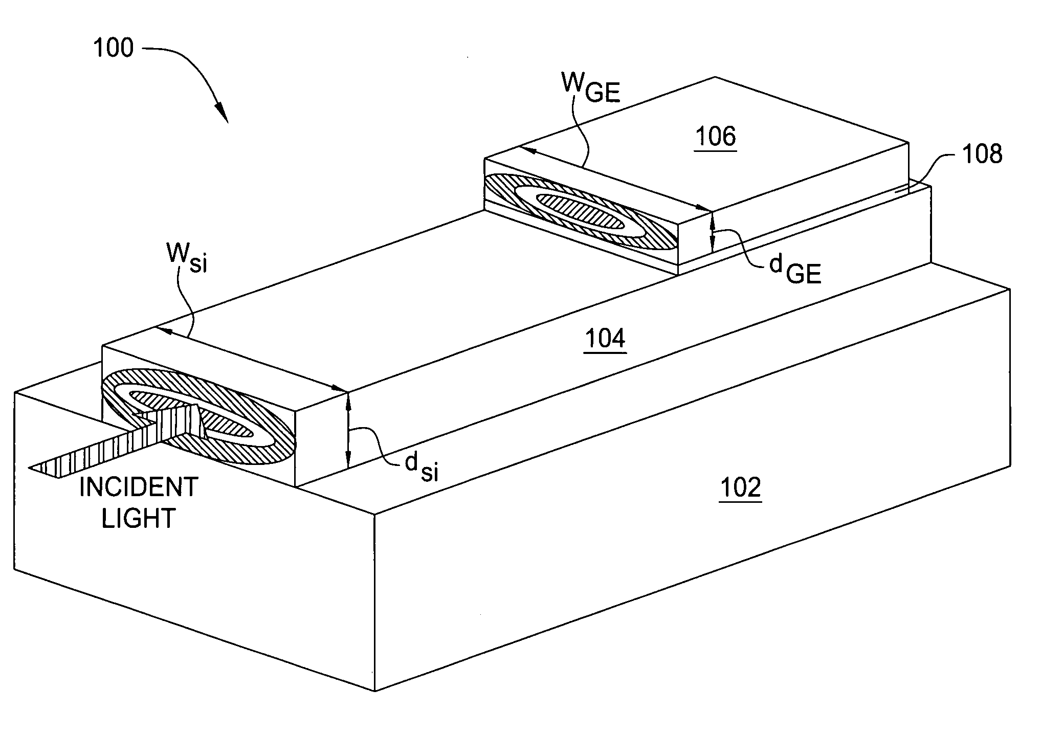
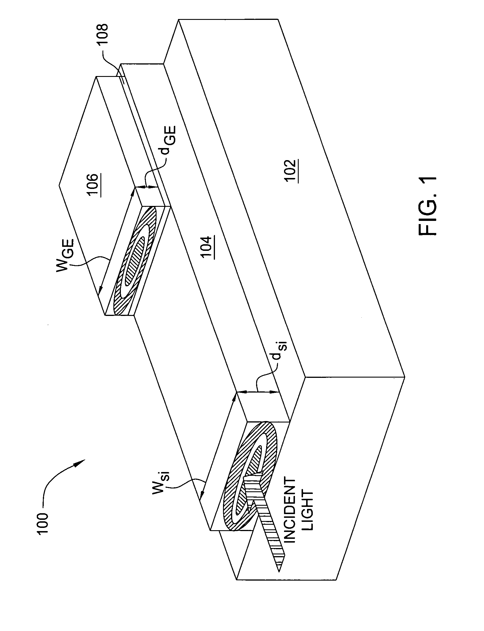
[0020]FIG. 2 is a perspective view of a waveguide photodetector 200, according to the present invention. Specifically, the photodetector 200 is an evanescently coupled waveguide photodetector. By “evanescently coupled”, it is meant that light is transmitted from the waveguide layer to the detection layer by means of the evanescent (or decaying) waves. This is typically accomplished by placing two or more waveguides close together so that the evanescent field does not decay much in the vicinity of the other waveguide. Assuming the receiving waveguide can support mode(s) of the appropriate frequency, the evanescent field gives rise to propagating wave mode(s), thereby connecting (or coupling) the wave from one waveguide to the next. As explained in greater detail below, the photodetector 200 exploits this concept of evanescent coupling in order to couple propagating light from a waveguide layer to a detection layer.

[0021] To this end, the photodetector 200 comprises a substrate 202, a...

third embodiment

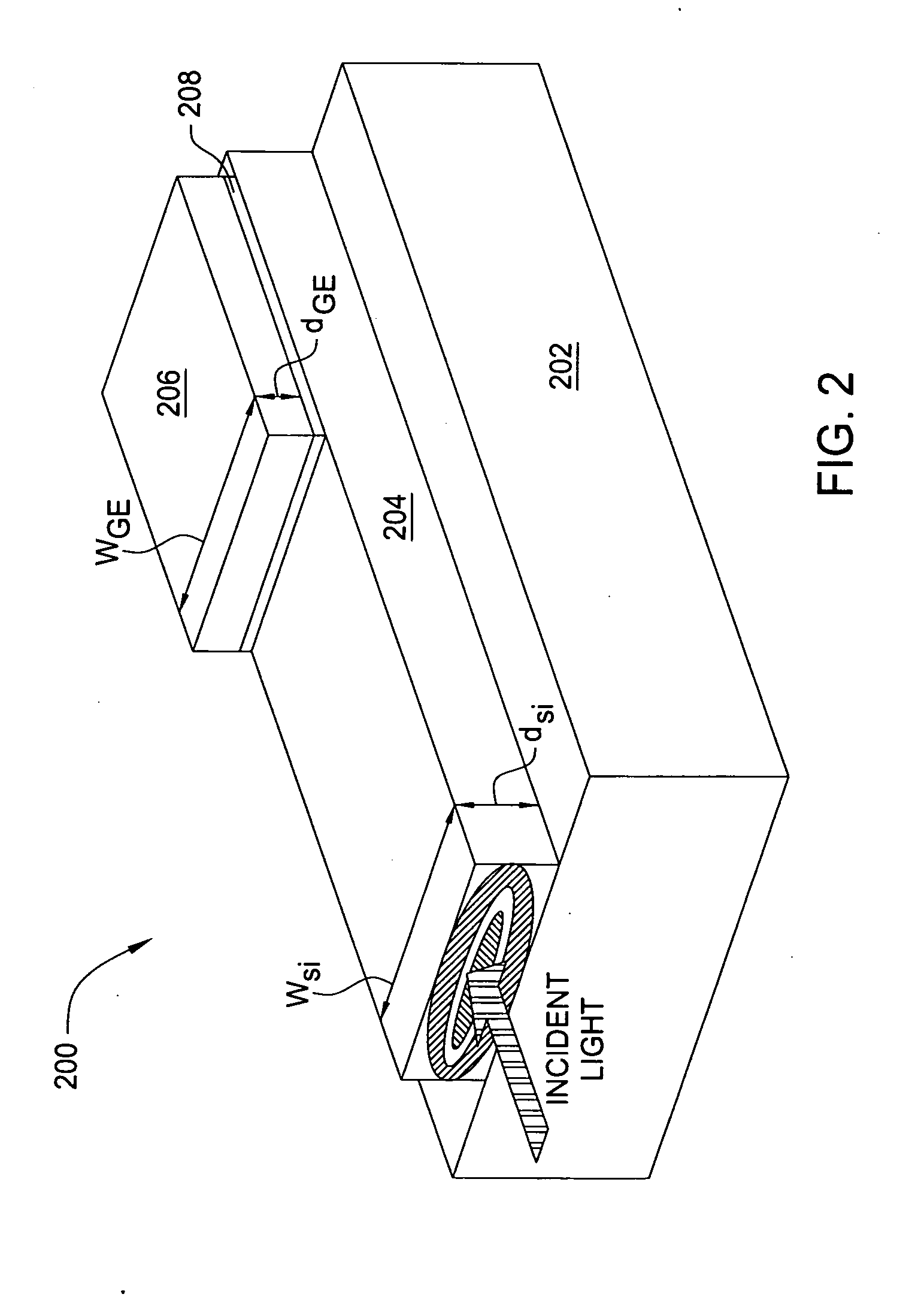
[0027]FIG. 3 is a perspective view of a waveguide photodetector 300, according to the present invention. Specifically, the photodetector 300 is a waveguide photodetector with an adiabatic taper coupler. To this end, the photodetector 300 comprises a substrate 302, a waveguide layer 304 formed on the substrate 302 and a detection layer 306 formed on the waveguide layer 304. Thus, in this embodiment, the waveguide layer 304 is effectively “sandwiched” between the substrate 302 and the detection layer 306. In alternative embodiments, however, the entire photodetector structure may be buried under a thick oxide layer, in which case there is no “sandwiching” of the waveguide layer 304.

[0028] The substrate 302 is an insulator. In one embodiment, the substrate 302 is a buried oxide substrate. The waveguide layer 304 is a single-mode strip waveguide in a wavelength of interest along its entire length. That is, the waveguide layer 304 provides, along its length, for the waveguiding of only a...


PUM


Abstract

The present invention is a waveguide photodetector. In one embodiment, the waveguide photodetector includes a waveguide layer where light is guided or is confined and a detection layer formed on the waveguide layer where guided light is detected. Each of the waveguide layer and the detection layer allows for the guiding of no more than a single mode of light for a given polarization. In another embodiment, the waveguide photodetector includes a waveguide layer where light is guided or is confined, a detection layer formed on the waveguide layer where guided light is detected, a first electrical contact coupled to the detection layer, and a second electrical contact coupled to the detection layer. The first electrical contact and the second electrical contact are disposed in a spaced-apart, substantially parallel manner relative to each other.

Description

BACKGROUND [0001] The invention relates generally to optical waveguides, and relates more particularly to waveguide photodetectors for converting optical signals into electrical signals. [0002] Optical interconnects can offer significant advantages over electrical circuitry in the field of advanced microelectronics. One possible implementation of a deeply-scaled optical interconnect system is based on silicon-on-insulator (SOI) technology, in which optical waveguides are formed (e.g., in accordance with CMOS technology) on a thin silicon device layer. Such a system requires four major components: a light source, an optical modulator for encoding data into light pulses, a waveguide for efficiently transporting light across the chip and a photodetector for converting optical signals into electrical signals. The lack of an effective photodetector for such applications has, however, impeded the development of highly scalable SOI interconnects to date. [0003] In particular, the photodete...

Claims


Application Information

Patent Timeline
Patent Type & Authority Applications(United States)
IPC IPC(8): G02B6/10G02B6/26
CPCH01L31/0232G02B6/12004H01L31/02327
Inventor DEHLINGER, GABRIELMCNAB, SHAREE J.VLASOV, YURII A.XIA, FENGNIAN
Owner IBM CORP
Why Eureka
Try Eureka