

Organic light emitting diode
- Summary
- Abstract
- Description
- Claims
- Application Information
AI Technical Summary
Benefits of technology
Problems solved by technology
Method used
Image

Examples
first embodiment
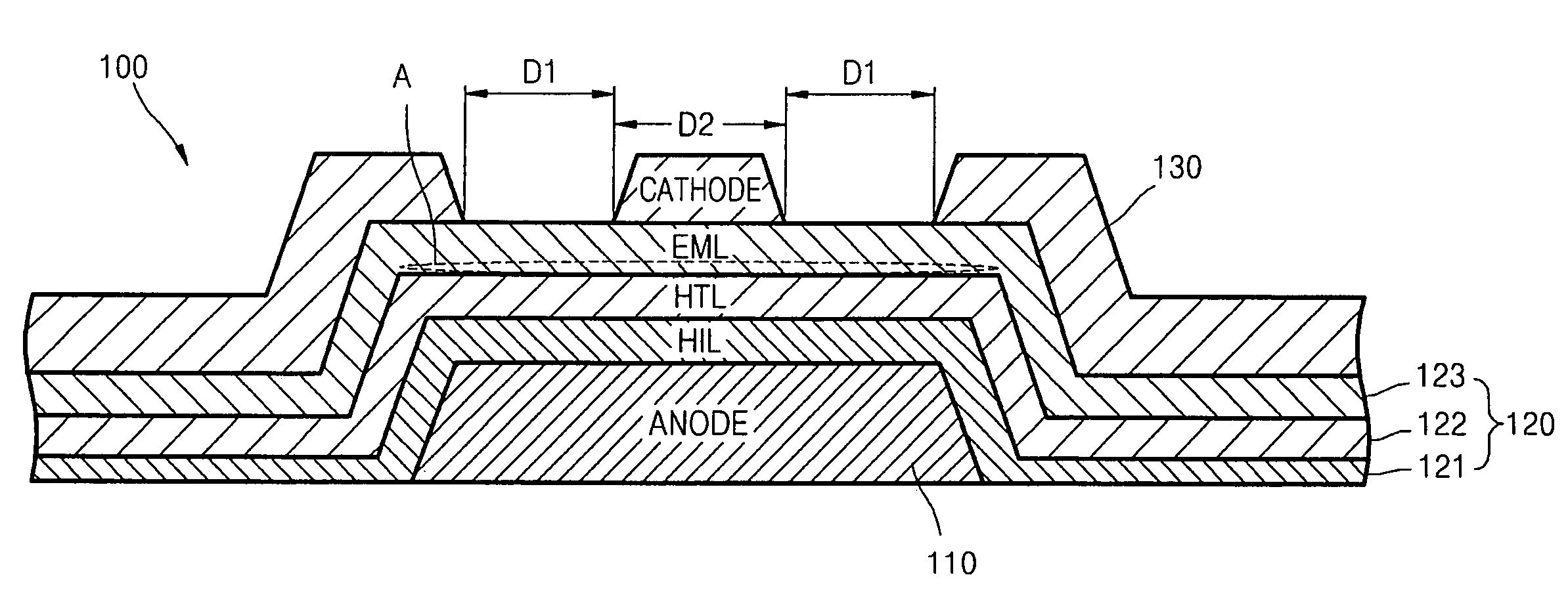
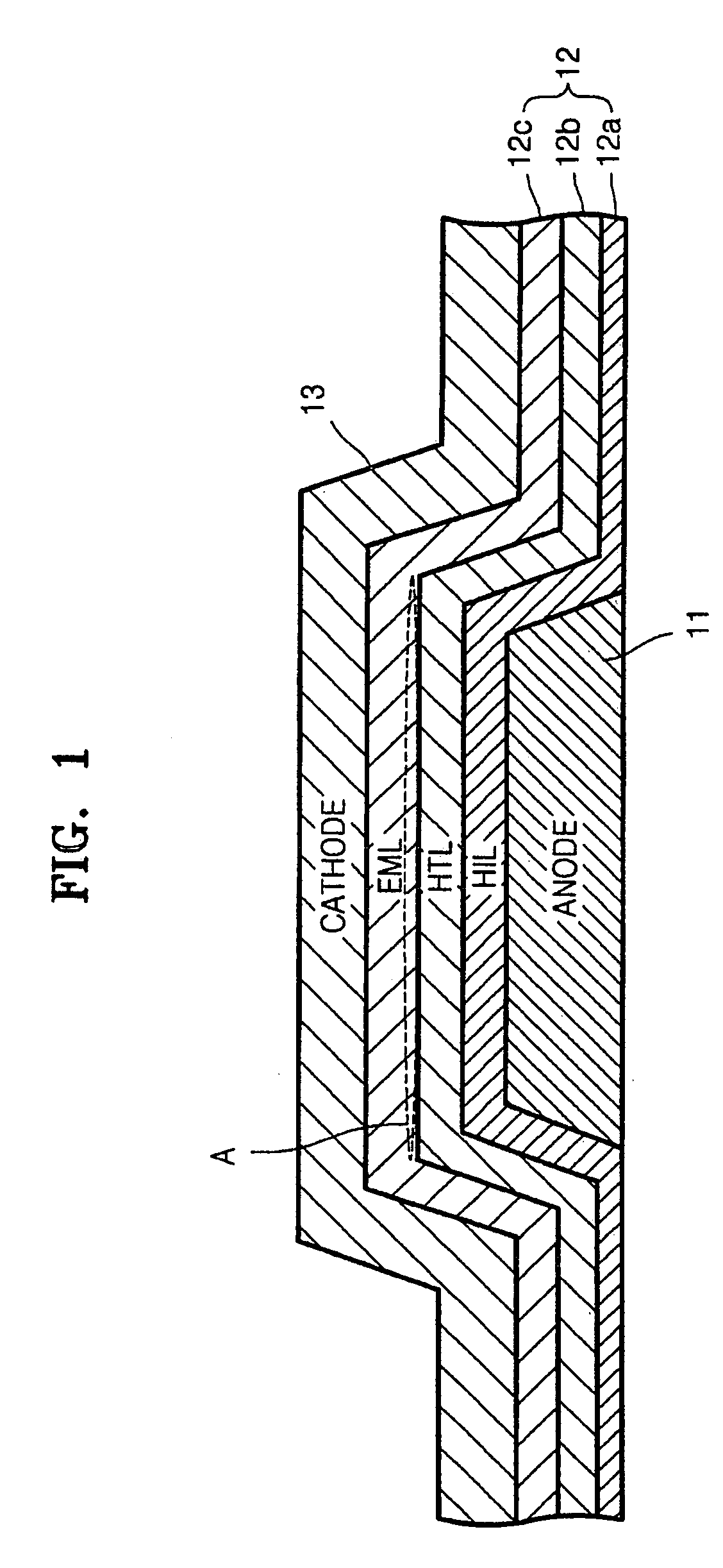
[0032]Turning now to FIG. 4, FIG. 4 is a cross sectional view of an organic light emitting diode 100 according to the present invention. As shown in FIG. 4, the organic light emitting diode 100 has a laminated structure including an anode 110, a light emitting part 120, and a cathode 130, which are arranged sequentially. The light emitting part 120 includes a hole injecting layer 121, a hole transporting layer 122, and a light emitting layer 123.
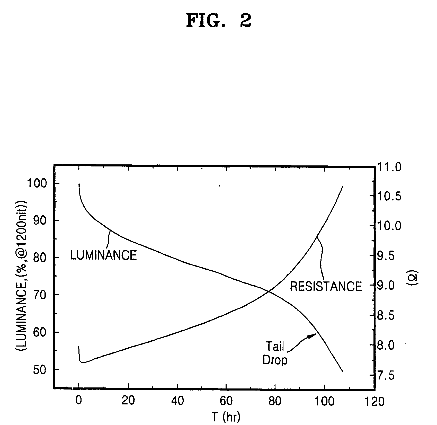
[0033]The cathode 130 does not entirely cover the light emitting part 120, and is formed in a striped pattern with a prong separation distance (pattern distance) D1 between each stripe or prong. According to an aspect of the present invention, the lifespan of the organic light emitting diode 100 is increased over that of FIG. 1 by exploiting edge light emission during the final usage stage. That is, during the initial usage stage, electric coupling is generated by electrons flowing along the straight arrows indicated in FIG. 5A between the c...
second embodiment
[0037]Turning now to FIG. 7, FIG. 7 is a cross-sectional view of an organic light emitting diode 200 according to the present invention. The organic light emitting diode 200 of FIG. 7 includes a cathode 230 having a continuous structure, and an anode 210 formed in a striped pattern with a prong separation distance D1. Even though separate light emitting passages for the initial and for the final usage stages are provided at the anode 210 instead of at the cathode 230, the light emission of OLED 200 of FIG. 7 is substantially equal to that of the OLED 100 of FIG. 4. In other words, an electric coupling occurs along a straight path directed to anode 210 during the initial usage stage, and along a curved path avoiding the deteriorated region during the final usage stage so that sufficient luminance can be achieved at each usage stage while increasing the the lifespan of the diode.
third embodiment
[0038]Turning now to FIG. 8, FIG. 8 is a cross-sectional view of an organic light emitting diode 300 according to the present invention. In the organic light emitting diode 300 of FIG. 8, both the anode 310 and the cathode 330 are formed in a striped pattern so that the prongs of the anode 310 partially overlap the prongs of the cathode 330. Accordingly, electric coupling can take place along a straight line during the initial usage stage and along a curved line during the final usage stage. Thus, different light emitting areas are used for each of the initial and the final usage stages and the lifespan of the diode can be increased.
[0039]Turning now to FIG. 9, FIG. 9 is a top view of the OLED 100 of FIG. 4 shows a top view of pronged cathode 130. As seen in FIG. 9, one possible two dimensional configuration of the cathode layer 130 is depicted, where prongs are separated from each other by a distance D1 and the middle prong has a width of D2. Alternatively, there can be many more p...
PUM
 Abstract
Description
Claims
Application Information