
Display device

Inactive Publication Date: 2007-08-23
SAMSUNG DISPLAY CO LTD
View PDF7 Cites 16 Cited by
  • Summary
  • Abstract
  • Description
  • Claims
  • Application Information

AI Technical Summary

Benefits of technology

[0010]In accordance with the exemplary embodiments thereof described herein, the present invention provides a driving apparatus for a display device that reduces the power consumption of the display device, and improves its response speed, reliability and durability.

Problems solved by technology

However, if a one-directional electric field is applied to the liquid crystal layer for a relatively long period of time, image degradation will occur.
Therefore, where the difference between the target voltage and the previously-charged voltage is large, if only the target voltage is initially applied, the pixel voltage may not reach the full target voltage during the time in which the pixel switching element is turned on.
The requirement for these elements creates problems in terms of circuit complexity and a concomitant increase in production costs.
However, because the resolution of medium-sized or small-sized LCDs is gradually increasing, the power consumption problem is also increasing.
In particular, when the DCC calculations are performed, the power consumption of the LCD is greatly increased, due to the additional calculation circuits required.
As a result, the desired luminance cannot be obtained.

Method used


Image

  • Display device
  • Display device
  • Display device

Examples


Embodiment Construction

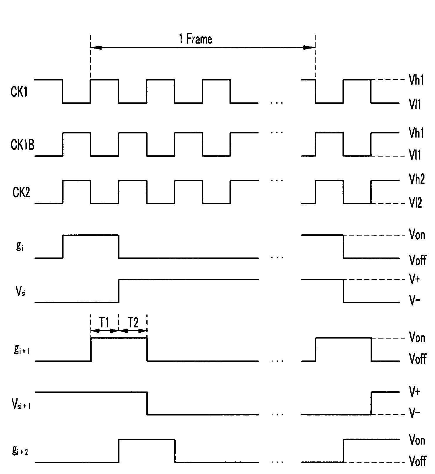
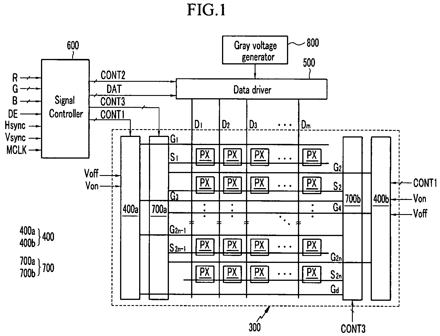
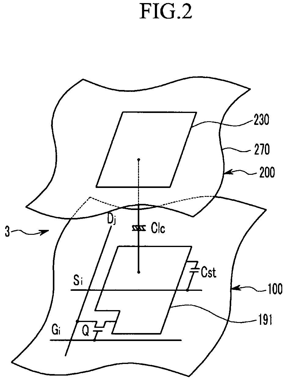
[0037]An exemplary embodiment of an LCD in accordance with the present invention is described in detail below with reference to FIGS. 1 and 2, wherein FIG. 1 is a functional block diagram of the exemplary LCD and FIG. 2 is a partial perspective view of an equivalent circuit diagram of a single pixel of the exemplary LCD.

[0038]As illustrated in FIG. 1, the exemplary LCD includes a liquid crystal panel assembly 300, a gate driver 400, a data driver 500, a gray voltage generator 800 connected to the data driver 500, a storage signal generator 700, and a signal controller 600 that controls these components.

[0039]The liquid crystal panel assembly 300, in terms of an equivalent circuit thereof, includes a plurality of signal lines G1-G2n, Gd, D1-Dm, and S1-S2n, and a plurality of pixels PX connected to the signal lines G1-G2n, Gd, D1-Dm, and S1-S2n and arranged substantially in the form of a rectangular matrix. In the schematic perspective structural view of FIG. 2, the liquid crystal pan...


PUM


Abstract

A display device includes gate lines, data lines, storage electrode lines and pixels. Each pixel includes a switching element connected to a gate line and a data line, a liquid crystal capacitor connected to the switching element and a common voltage, and a storage capacitor connected to the switching element and a storage electrode line. Signal generating circuits of the display generate storage signals based on gate signals in such a way that the storage signal applied to each pixel has a changed voltage level immediately after the completion of the charging of the data voltage into the liquid crystal capacitor and the storage capacitor. This enables the pixel electrode to reach the target voltage in a single frame, reduces the power consumption of the display, and improves its response time, reliability and durability.

Description

RELATED APPLICATION[0001]This application claims priority of Korean Patent Application No. 10-2006-0016270, filed Feb. 20, 2006, the entire disclosure of which is incorporated herein by reference.BACKGROUND[0002]This present invention relates to display devices, such as liquid crystal displays (LCDs) s.[0003]In general, an LCD includes two display panels having pixel electrodes and a common electrode, and a layer of a liquid crystal material having dielectric anisotropy interposed therebetween. The pixel electrodes are arranged in a matrix and connected to switching devices, such as thin film transistors (TFTs), which sequentially apply data voltages to them on a row-by-row basis. The common electrode is disposed over the entire surface of the display panel and has a common voltage applied it. The pixel electrode, the common electrode, and the liquid crystal layer interposed therebetween constitute a liquid crystal capacitor. The liquid crystal capacitor, together with the switching...

Claims


Application Information

Patent Timeline
IPC IPC(8): G09G3/36
CPCG09G3/3614G09G3/3655G09G2300/0876G09G2330/021G09G2310/08G09G2320/0252G09G2310/0281E02D5/808E02D2250/0023E02D2600/30
Inventor CHOI, JIN-YOUNGJEON, JIN
Owner SAMSUNG DISPLAY CO LTD
Features
  • Generate Ideas
  • Intellectual Property
  • Life Sciences
  • Materials
  • Tech Scout
  • Unparalleled Data Quality
  • Higher Quality Content
  • 60% Fewer Hallucinations
Learn More