High power semiconductor laser device

a laser device and high-power technology, applied in semiconductor lasers, lighting and heating devices, furniture, etc., can solve the problems of reducing affecting the practical application, and affecting the efficiency of optical output, so as to reduce the internal optical loss and increase the length

Active Publication Date: 2007-08-23
SAMSUNG ELECTRONICS CO LTD
View PDF3 Cites 29 Cited by
  • Summary
  • Abstract
  • Description
  • Claims
  • Application Information

AI Technical Summary

Benefits of technology

[0014]The present invention has been made to solve the foregoing problems of the prior art and therefore an aspect of the present invention is to provide a high power semiconductor laser device capable of confining higher order mode occurrence and reducing internal optical loss in order to design a resonator with a greater length.

Problems solved by technology

However, the resonator with a greater length L disadvantageously degrades optical output efficiency due to internal optical loss [cm−1] of the resonator.
However, in a case where the optical guide layers are increased in thickness to decrease internal optical loss, it may trigger a higher order mode beam, seriously distorting beam shape and causing mismatch with an optical system.
This poses difficulty to practical application thereof.
Consequently, in the conventional semiconductor laser device, the resonator is limitedly prolonged in its length to enhance output owing to such internal optical loss problems.

Method used


Image

  • High power semiconductor laser device
  • High power semiconductor laser device
  • High power semiconductor laser device

Examples


Embodiment Construction

[0028]Exemplary embodiments of the present invention will now be described in detail with reference to the accompanying drawings.

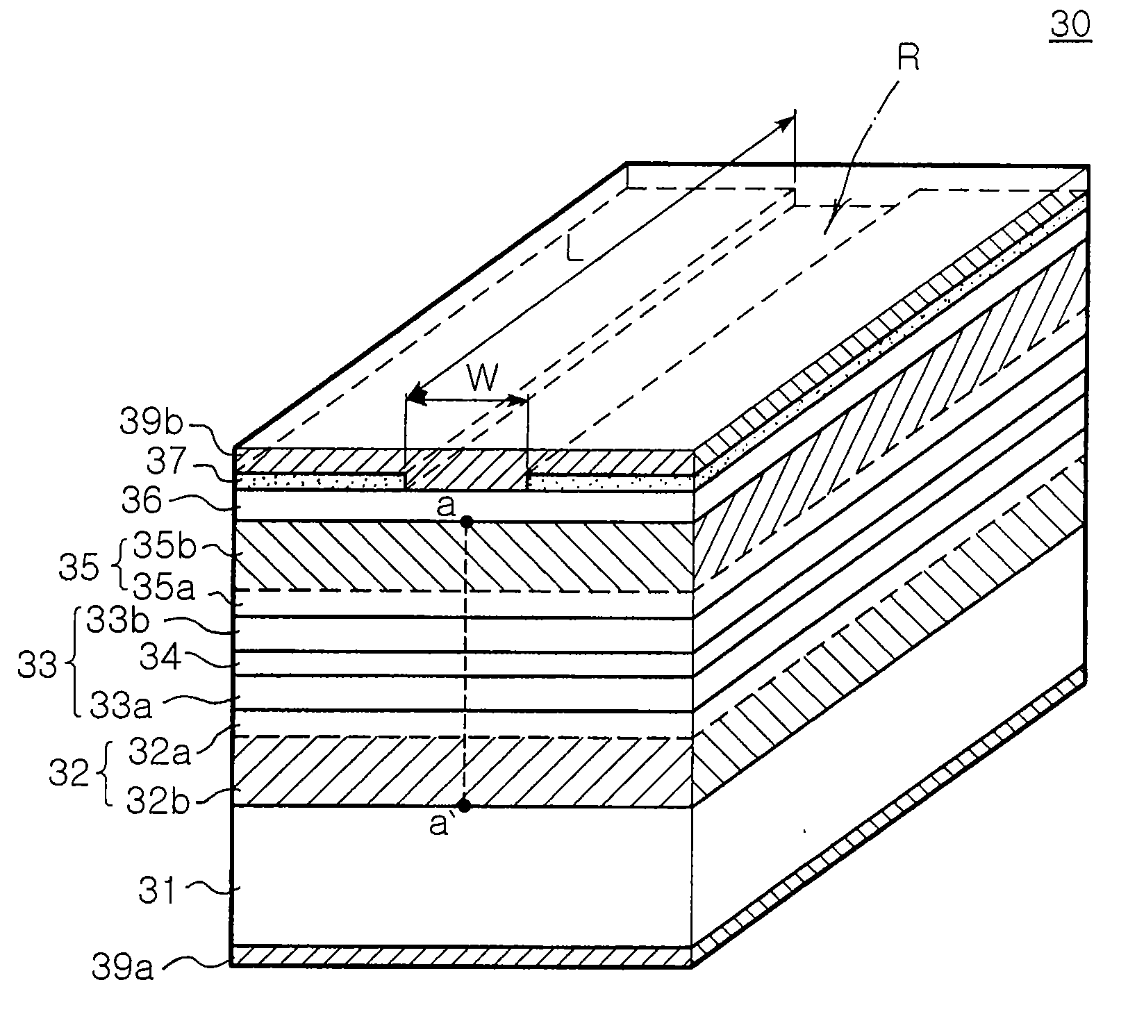
[0029]FIG. 3 is a schematic perspective view illustrating a high power semiconductor laser device according to an embodiment of the invention.

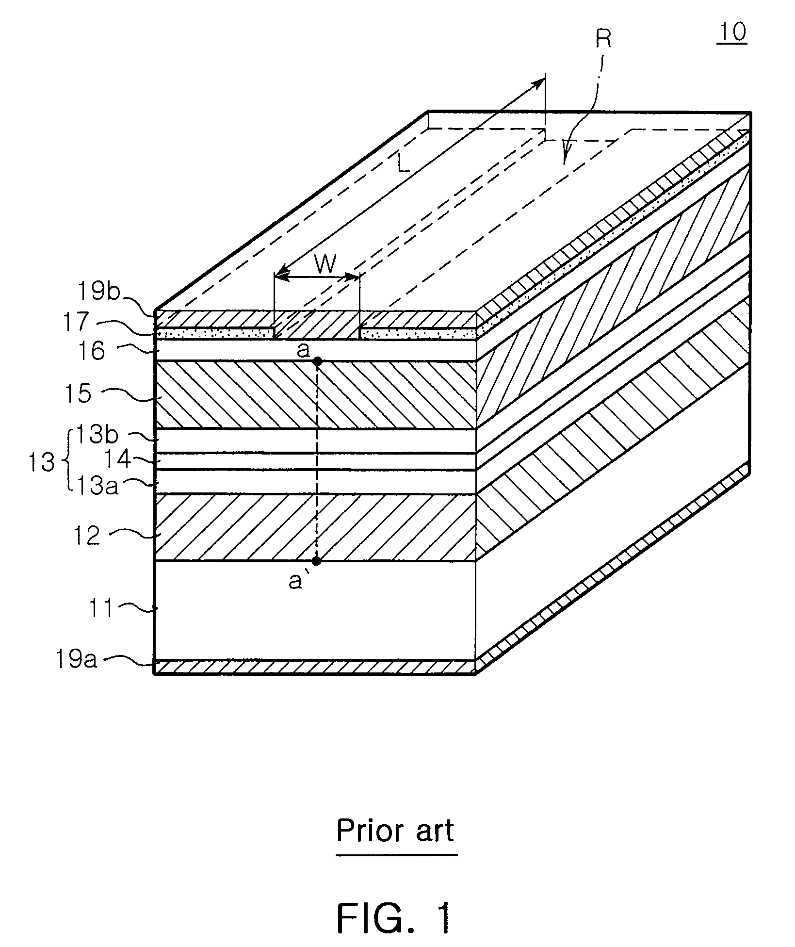
[0030]Referring to FIG. 3, the high power semiconductor laser device 30 includes first and second conductivity type clad layers 32 and 35 formed on a conductive substrate 31 and an active layer 34 interposed therebetween. A first undoped clad layer 32a is disposed between the first conductivity type clad layer 32 and the active layer, and a second undoped clad layer 35a is disposed between the second conductivity type clad layer 35 and the active layer 34. First and second optical guide layers 33a and 33b are undoped layers having higher reflectivity than the first and second conductivity type clad layers 32 and 35 and the first and second undoped clad layers 32a and 35a, respectively. The first and second optical gu...


PUM


Abstract

In a high power semiconductor laser device, first and second conductivity type clad layers are provided. An active layer is interposed between the first and second conductivity type clad layers. A first optical guide layer is disposed between the first conductivity type clad layer and the active layer. A second optical guide layer is disposed between the second conductivity clad layer and the active layer. Also, an intentionally undoped optical loss confinement region is formed in a portion of at least one of the first and second conductivity type clad layers overlapping laser beam distribution.

Description

CLAIM OF PRIORITY[0001]This application claims the benefit of Korean Patent Application No. 2006-17419 filed on Feb. 22, 2006 in the Korean Intellectual Property Office, the disclosure of which is incorporated herein by reference.BACKGROUND OF THE INVENTION[0002]1. Field of the Invention[0003]The present invention relates to a high power semiconductor laser device, more particularly, which has superb optical output efficiency due to decreased internal optical loss.[0004]2. Description of the Related Art[0005]Recently, a high power semiconductor laser device has found its various applications, for example, in an industrial field such as optical telecommunication, optical recording devices, welding and cutting and in a medical field. The high power semiconductor laser device is also being used as a visible ray laser for displays, with a prospect for growth in its application in the future.[0006]In general, the semiconductor laser device can have high output characteristics by virtue o...

Claims


Application Information

Patent Timeline
Patent Type & Authority Applications(United States)
IPC IPC(8): H01S5/00
CPCH01S5/0425H01S5/2022H01S5/2004H01S5/20H01S5/04256F26B3/347F26B2200/04
Inventor MA, BYUNG JINBAE, SEONG JU
Owner SAMSUNG ELECTRONICS CO LTD
Why Eureka
Try Eureka