Method and apparatus for forming bumps for semiconductor interconnections using a wire bonding machine

a technology of wire bonding machine and semiconductor, which is applied in the direction of soldering apparatus, semiconductor/solid-state device details, instruments, etc., can solve the problems of damage to surrounding circuitry, inability to form stitch bonding on bond pads, damage to circuitry on dies, etc., to achieve the effect of reducing the clearance and minimizing the sag of wires

Inactive Publication Date: 2007-08-30
KULICKE & SOFFA IND INC
View PDF21 Cites 25 Cited by
  • Summary
  • Abstract
  • Description
  • Claims
  • Application Information

AI Technical Summary

Benefits of technology

[0020] Preferably the capillary is positioned for the final diagonal motion so that the tip of the capillary contacts and smooths a portion of the top of the bump. This technique can form a taller and larger bump to provide increased clearance for both flip chip applications and reverse wire bonding applications. For reverse wire bonding application, the first lateral motion preferably is in a direction toward the site of the other end of the wire loop (i.e., where the first / ball bond of the completed loop will be formed) so that the sloped, smooth surface on top of the bump where the stitch bond wilt be formed slopes upwardly toward the direction of the wire loop. This arrangement provides a sloped surface that minimizes wire sag near the stitch bond by causing the wire to have more of an upward angle at the stitch bond.

Problems solved by technology

If the capillary contacts the top of a die, it likely will damage circuitry on the die.
Nevertheless, it is sometimes desirable to make a stitch bond on a die.
However, it usually would not be possible to form a stitch bond on a bond pad on a die for the reasons discussed above, namely, the capillary might damage surrounding circuitry on the die. when it contacts the die to form the stitch bond.
Further, packages are becoming thinner and thinner.
Accordingly, present techniques for reverse bonding are becoming less and less effective.
Particularly, it is becoming increasingly difficult in reverse bonding to achieve sufficient height clearance of the wire loops to reasonably assure that the wires will not contact the top or edge of the die or adjacent wires.
Also, with smaller and smaller bumps, it is becoming increasingly difficult to form reliable stitch bonds on top of the bumps.
However, with very fine wires and / or fine pitch applications, it is still difficult with this technique to assure adequate clearance between the wire and the die.
Particularly, while the purely lateral smoothing motion worked well for many applications, it was found that, as ball sizes and pitches continued to decrease in size, the force exerted by the capillary tip on the bump during the purely lateral smoothing motion could tear the bump off of the pad.
In either embodiment, since a portion of the top of the bump was being scraped off, this technique often suffered even greater problems of inadequate clearance.
As wire diameters and pitches of the bond pads continue to decrease, it is becoming more and more difficult to form bumps of sufficient height and uniformity with a wire bonding machine.

Method used


Image

  • Method and apparatus for forming bumps for semiconductor interconnections using a wire bonding machine
  • Method and apparatus for forming bumps for semiconductor interconnections using a wire bonding machine
  • Method and apparatus for forming bumps for semiconductor interconnections using a wire bonding machine

Examples


Embodiment Construction

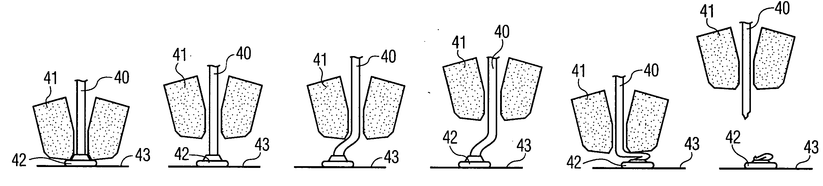
[0037]FIGS. 4A through 4F generally illustrate the position of the capillary tip and the wire at six different stages of an exemplary bump formation process in accordance with the present invention. As shown, the beginning of the bump formation process is essentially identical to the prior art techniques. Particularly, the process starts with a short distance of the wire 40 extending from the capillary 41. The wire is hit with an electric spark to cause it to melt and inherently form into a ball 42. The capillary then drops down to contact the bond site 43 and squeeze the ball against the surface of the bond site and form the initial shape of the bump as dictated by the shape of the capillary tip. Heat and / or ultrasonic energy is applied to form the bond between the ball and the surface. FIG. 4A shows the process at this point.

[0038] Next, the capillary 41 rises with the clamps (not shown) open in order to pay out a short distance of wire extending from the top of the bonded ball 4...


PUM

PropertyMeasurementUnit
heightaaaaaaaaaa
lateral distanceaaaaaaaaaa
energyaaaaaaaaaa

Abstract

The present invention is a method and apparatus for forming a bump for semiconductor interconnect applications, such as reverse wire bonding or stud bumping for flip chip interconnections. The bump is formed by (1) ball bonding at the bump site, (2) raising the capillary a predetermined height after forming the ball bond with the wire paying out of the capillary tip, (3) moving the capillary laterally a predetermined distance, preferably in a direction toward the site of other end of the wire loop, if the bump is to be used as the platform for a stitch bond of a wire loop, (4) raising the capillary further, and (5) moving the capillary diagonally downwardly and in the opposite direction of the first lateral motion. The wire is then severed by raising the capillary, closing the clamps and raising the capillary again to snap the wire pigtail off at the bump.

Description

CROSS-REFERENCE TO RELATED APPLICATIONS [0001] This application is a Divisional of U.S. patent application Ser. No. 10 / 247,242, filed Sep. 19, 2002, the disclosure of which is incorporated herein by reference.FIELD OF THE INVENTION [0002] The invention pertains to semiconductor electrical interconnection techniques. More particularly, the invention pertains to the formation of bumps for semiconductor interconnections using a wire bonding machine. BACKGROUND OF THE INVENTION [0003] There are numerous techniques in common usage for forming the electrical interconnections between the bond pads of a semiconductor die and a lead frame or other substrate. One of the oldest and still most common techniques is to form a wire bond between a die and its substrate using a wire bonding machine. The wire bonding machine forms a wire through the air between the die bond pad and the appropriate electrical connection point on the substrate (e.g., a lead finger of a lead frame). [0004] A typical wir...

Claims


Application Information

Patent Timeline
Patent Type & Authority Applications(United States)
IPC IPC(8): B23K3/00G06F19/00H01L21/60H01L21/607
CPCH01L24/11H01L2924/01033H01L24/45H01L24/48H01L24/78H01L24/85H01L2224/13099H01L2224/45144H01L2224/48091H01L2224/48095H01L2224/48227H01L2224/48465H01L2224/48471H01L2224/48479H01L2224/48599H01L2224/78301H01L2224/786H01L2224/85051H01L2224/851H01L2224/85181H01L2224/85186H01L2224/85205H01L2224/85986H01L2924/01004H01L2924/01005H01L2924/01006H01L2924/01079H01L2924/01082H01L2924/14H01L24/12H01L2924/00014H01L2924/00H01L24/13H01L2224/1134H01L2224/13144H01L2224/45015H01L2224/48228H01L2924/00015H01L2924/20752H01L2924/20753H01L2924/20755H01L2924/20754H01L2924/2075H01L2224/4554H01L2224/85399H01L2224/05599
Inventor BABINETZ, STEPHENTSUJIMURA, TAKASHIOHTSUBO, HIROYUKIMORIMOTO, YASUHIRO
Owner KULICKE & SOFFA IND INC
Why Eureka
Try Eureka