Semiconductor memory device and memory system including the same

a memory device and semiconductor technology, applied in the field of semiconductor memory devices, can solve the problems of increasing the layout area affecting the performance of conventional semiconductor memory devices, so as to achieve the effect of increasing the layout area and not degrading the ability to detect errors

Active Publication Date: 2007-08-30
SAMSUNG ELECTRONICS CO LTD
View PDF11 Cites 38 Cited by
  • Summary
  • Abstract
  • Description
  • Claims
  • Application Information

AI Technical Summary

Benefits of technology

[0012]An example embodiment may provide a semiconductor memory device capable of generating an error detection code without degrading error detection ability and without increasing a layout area.

Problems solved by technology

This not only increases the layout area of conventional semiconductor memory devices but also delays signal transmission due to increased length of the signal line or lines used to provide the data DO1, DO2, DO3 and DO4 to the error detection code generator.
Similar problems still in occur in conventional semiconductor memory devices even if the error detection code generator is disposed in a region B between regions where the memory cell array blocks BLK1 and BLK2 are disposed or in a region C between regions where the memory cell array blocks BLK3 and BLK4 are disposed.

Method used


Image

  • Semiconductor memory device and memory system including the same
  • Semiconductor memory device and memory system including the same
  • Semiconductor memory device and memory system including the same

Examples


Embodiment Construction

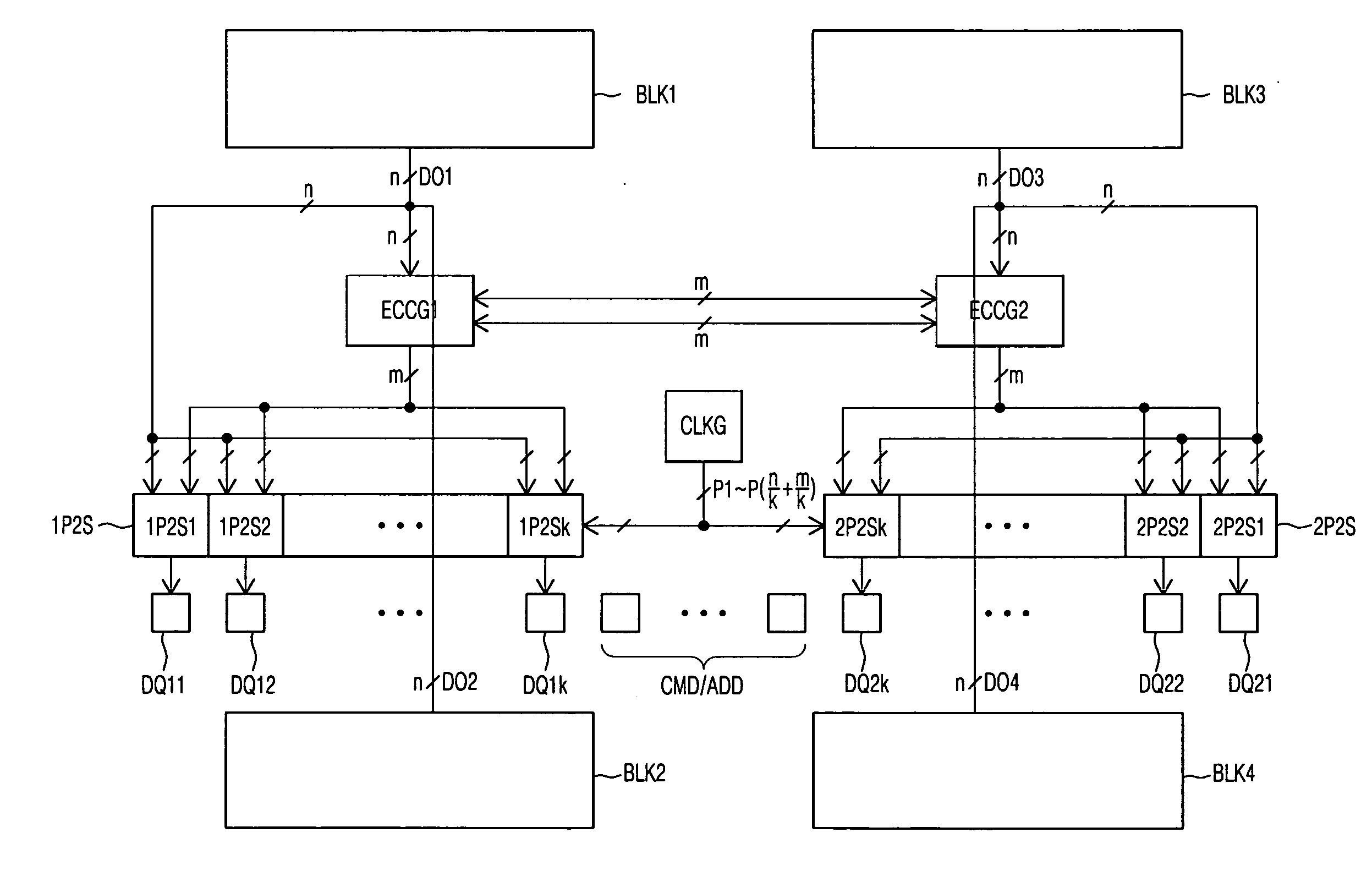
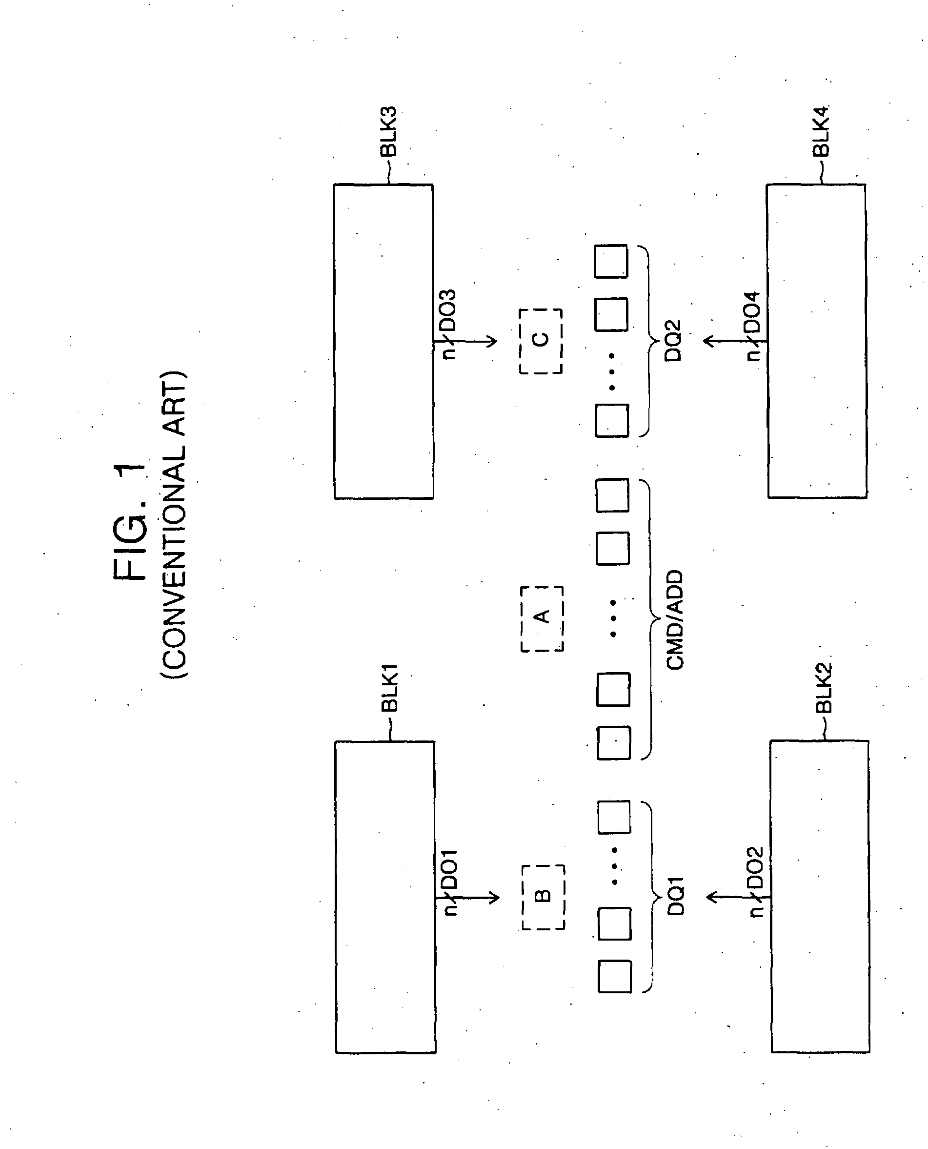
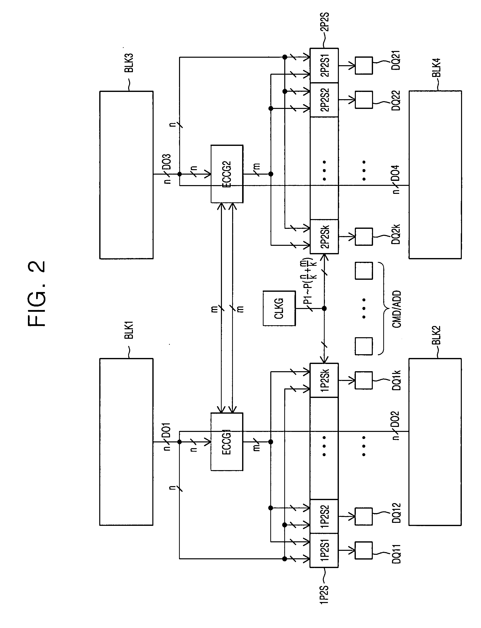
[0040]Various example embodiments will now be described more fully with reference to the accompanying drawings in which some example embodiments are shown. Detailed example embodiments are disclosed herein. However, specific structural and functional details disclosed herein are merely representative for purposes of describing example embodiments, and one skilled in the art will appreciate that example embodiments may be embodied in many alternate forms and should not be construed as limited to only the embodiments set forth herein.

[0041]Accordingly, while example embodiments are capable of various modifications and alternative forms, example embodiments are shown by way of example in the drawings and are described in detail below. It should be understood, however, that there is no intent to limit example embodiments to the particular forms disclosed, but on the contrary, example embodiments are to cover all modifications, equivalents, and alternatives falling within the scope of th...


PUM


Abstract

A semiconductor memory device and a memory system including the same are provided. The semiconductor memory device may include a first memory cell array block generating first data, a second memory cell array block generating second data, and first and second error detection code generators. The first error detection code generator may generate a first error detection code and may combine a portion of bits of the first error detection code with a portion of bits of a second error detection code to generate a first final error detection signal. The second error detection code generator may generate the second error detection code and may combine the remaining bits other than the portion of bits of the second error detection code with the remaining bits other than the portion of bits of the first error detection code to generate a second final error detection signal.

Description

PRIORITY STATEMENT[0001]This application claims the benefit of Korean Patent Application No. 2006-13898, filed Feb. 13, 2006, the entire contents of which is incorporated herein by reference.BACKGROUND OF THE INVENTION[0002]1. Field of the Invention[0003]Example embodiments relate to a semiconductor memory device, and more particularly, to a semiconductor memory device having an Outer Data Inner Control (ODIC) pad structure and a memory system including the same.[0004]2. Description of the Related Art[0005]A conventional semiconductor memory device having an ODIC pad structure has a structure in which data pads are disposed at both sides thereof and a command pad is disposed at an inner side thereof. Data input and output via the data pad disposed at one side may be input and output through only a memory cell array block disposed at one side, and data input and output via the data pad disposed at the other side may be input and output through only a memory cell array block disposed ...

Claims


Application Information

Patent Timeline
Patent Type & Authority Applications(United States)
IPC IPC(8): G11C29/00
CPCG06F11/1008G11C7/1006G11C29/42H03M13/29G11C2207/104G06F11/08G11C2029/0411G01M99/007G01N3/08G01N2203/0019H01R11/22
Inventor CHUNG, HOE-JUKIM, KYU-HYOUN
Owner SAMSUNG ELECTRONICS CO LTD
Why Eureka
Try Eureka