Versatile system for optimizing current gain in bipolar transistor structures

a bipolar transistor and current gain technology, applied in the field of semiconductor device fabrication and operation, can solve the problems of low efficiency, low efficiency, and inability to optimize current gain in bipolar transistors, and achieve the effect of reducing or eliminating hfe variation in bipolar transistors, improving device switching speed and overall device performance and reliability, and ensuring efficient optimization and maximization of h

Inactive Publication Date: 2007-09-06
INTEL CORP
View PDF23 Cites 1 Cited by
  • Summary
  • Abstract
  • Description
  • Claims
  • Application Information

AI Technical Summary

Benefits of technology

[0007] A system that provides Hfe optimization during circuit design, particularly for bipolar transistor structures, while comprehending peculiar physical properties and effects of small geometry manufacturing processes, is now needed. This system should decrease or eliminate Hfe variation in bipolar transistors—providing efficient optimization and maximization of Hfe, thereby improving device switching speed and overall device performance and reliability.

Problems solved by technology

In order for mass-production technologies to be cost-effective, tight parametric control of individual circuits must, to some extent, be compromised.
High speed, high volume processing cannot be stopped or slowed to analyze or correct unique, design-related, parametric variations.
Often, parametric variations across disparate circuit designs are not addressed during processing, and not identified until finished devices are tested or fail in use.

Method used


Image

  • Versatile system for optimizing current gain in bipolar transistor structures
  • Versatile system for optimizing current gain in bipolar transistor structures
  • Versatile system for optimizing current gain in bipolar transistor structures

Examples


Embodiment Construction

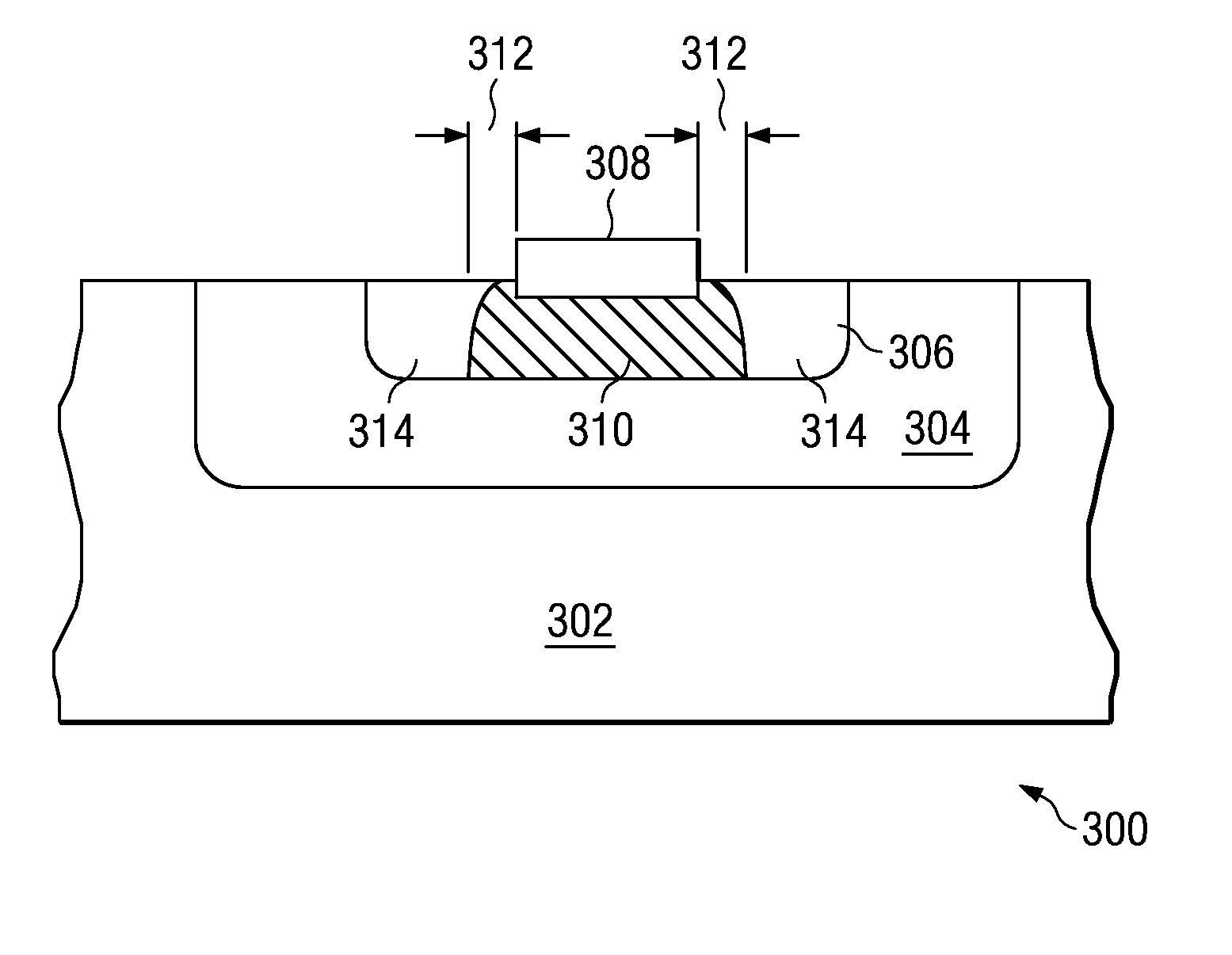
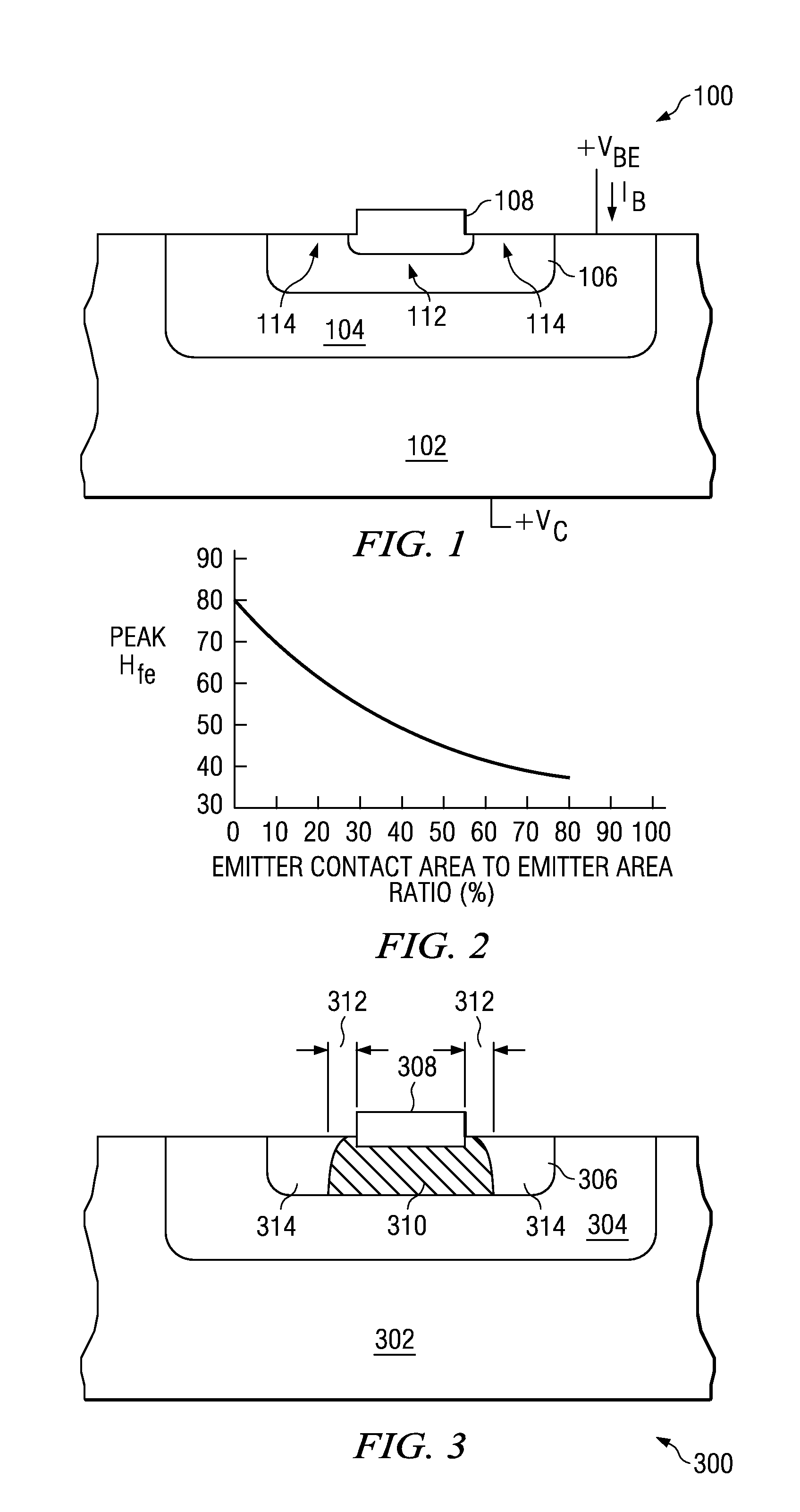
[0016] The present invention defines a system, comprising various structures and methods, for optimizing the current gain (Hfe) of bipolar structures during device design. The present invention comprehends the sensitivity of Hfe to the ratio of emitter contact area v. emitter area, accounting for this sensitivity by providing a system of contact design that maximizes Hfe for a given contact area.

[0017] It should be understood that the principles disclosed herein may be applied in a wide range of semiconductor processing applications. Specifically, the present invention may be applied to any number of situations where the current gain of diffused bipolar structures, particularly those in shallow device geometry technologies, is of concern. For purposes of explanation and illustration, however, the present invention is hereafter described in reference to an emitter structure in a BiCMOS transistor device.

[0018] As semiconductor device geometries are continually scaled downward, crit...


PUM


Abstract

Disclosed are apparatus and methods for designing electrical contact for a bipolar emitter structure. The area of an emitter structure (106, 306, 400, 404) and the required current density throughput of an electrical contact structure (108, 308, 402, 406) are determined. A required electrical contact area is determined based on the required current density, and the electrical contact structure is then designed to minimize the required electrical contact area with respect to the emitter structure area.

Description

[0001] This application is a divisional of application Ser. No. 10 / 196,634, filed Jul. 15, 2002, which claims the benefit of provisional Application No. 60 / 344,664, filed Dec. 28, 2001. FIELD OF THE INVENTION [0002] The present invention relates in general to the fabrication and operation of semiconductor devices and, more particularly, to devices and methods for optimizing current gain in semiconductor devices utilizing bipolar transistor structures. BACKGROUND OF THE INVENTION [0003] This application claims priority from Provisional Application Ser. No. 60 / 344,664, filed on Dec. 28, 2001. [0004] The continual demand for enhanced integrated circuit performance has resulted in, among other things, a dramatic reduction of semiconductor device geometries, and continual efforts to optimize the performance of every substructure with any semiconductor device. A number of improvements and innovations in fabrication processes, material composition, and layout of the active circuit levels o...

Claims


Application Information

Patent Timeline
Patent Type & Authority Applications(United States)
IPC IPC(8): H01L29/739H01L21/331H01L21/8249H01L29/08
CPCH01L21/8249H01L29/66272H01L29/0804
Inventor TROGOLO, JOECHATTERLEE, TATHAGATASPRINGER, LILYSMITH, JEFF
Owner INTEL CORP
Why Eureka
Try Eureka