Data storage nanostructures

a nano-structure, data technology, applied in nanotechnology, magnetic recording, mechanical recording, etc., can solve the problems of affecting the dense packing expected from the use of nano-structures, extending the structure in the horizontal direction of the substrate wafer, and poor memory function at temperatures above cryogenicity

Inactive Publication Date: 2007-09-06
QUNANO
View PDF49 Cites 43 Cited by
  • Summary
  • Abstract
  • Description
  • Claims
  • Application Information

AI Technical Summary

Benefits of technology

[0018] A further advantage of the invention is that a wide range of ma

Problems solved by technology

Prior art MJT memories typically exhibit small energy barriers, resulting in poor memory function at temperatures above the cryogenic.
Another drawback with the prior art single electron memory structures is that the structures extends in the horizontal direction of the substrate wafer.
Together with electrodes connecting to the MJTs the assemblies ex

Method used


Image

  • Data storage nanostructures
  • Data storage nanostructures
  • Data storage nanostructures

Examples


Embodiment Construction

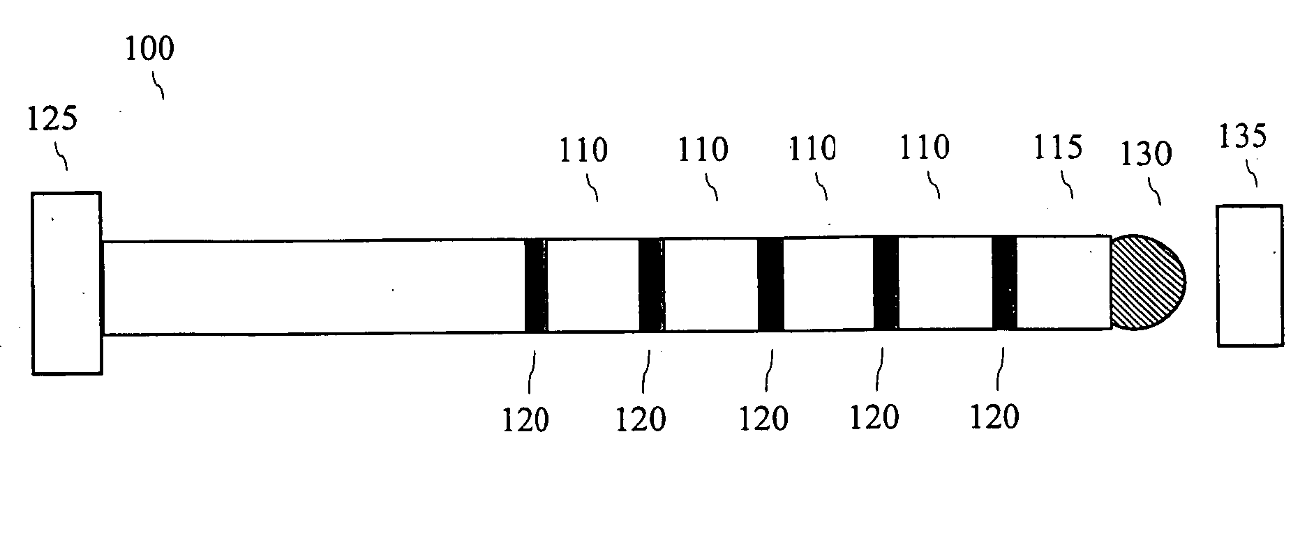
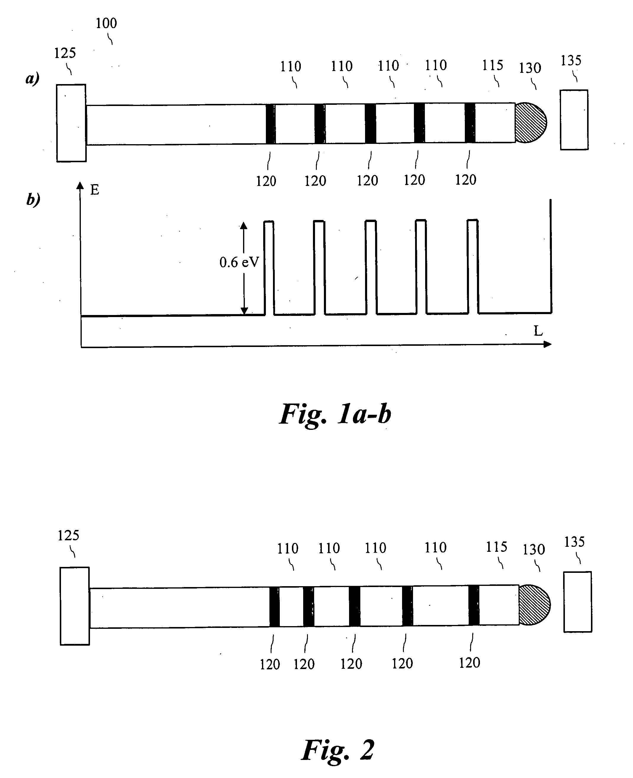
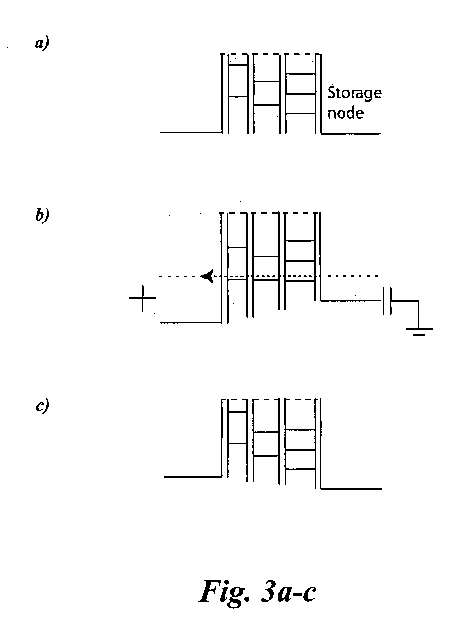
[0030] Multi-tunnel junctions are of interest for memories as they can be used to store electrons. The major technological problem is, as described in the background section, to fabricate a sufficient number of tunnel barriers in a reproducible way, where the device should have as low stray capacitances as possible. According to the present invention a single electron memory device is provided comprising of at least one heterostructured nanowhisker as the charge storing component. Each nanowhisker comprises a sequence of axial segments of materials of different band gaps, whereby to provide a sequence of conductive islands separated by tunnel barriers, whereby to provide a data storage capability. A memory assembly according to the invention is formed by a plurality of vertically standing nanowhiskers, i.e. the base ends of the nanowhisker essentially defining one plane and the top ends defining a second plane elevated above the first plane. Thus a very dense packing of the nanowhis...


PUM


Abstract

The present invention relates to a device for data storage. In particular the invention relates to a single electron memory device utilizing multiple tunnel junctions, and arrays or matrixes of such devices. The data storage device according to the invention comprises at least one nanowhisker adapted to store a charge. Each of the nanowhiskers comprises a sequence of axial segments of materials of different band gaps, arranged to provide a sequence of conductive islands separated by tunnel barriers and a storage island arranged at one end of the conductive island/tunnel barrier sequence, whereby to provide a data storage capability. The number of conductive islands should preferably be between five and ten.

Description

FIELD OF THE INVENTION [0001] The present invention relates to a device for data storage. In particular the invention relates to a single electron memory device utilizing multiple tunnel junctions, and arrays or matrixes of such devices. BACKGROUND OF THE INVENTION [0002] The interest in single electron device, and in particular single electron memories, has over the last couple of years shown an significant increase. [0003] The interest, for the data storage applications, arising primarily from the seemingly ever increasing demand for faster and more densely packed memories in combination with recent reports indicating that such memories are technologically achievable. Compared to the today most used nonvolative memories for handheld devices, flash memories, memories based on single-electron devices have the potential of offering extremely dense memories since the devices are of nanoscale dimensions. Another advantage is very low power consumption due to the fact that only a very l...

Claims


Application Information

Patent Timeline
IPC IPC(8): G11B5/00
CPCB82Y10/00G11C16/02G11C2216/08H01L29/0665Y10S977/943H01L29/068H01L29/8616Y10S977/902H01L29/0673
Inventor THELANDER, CLAESSAMUELSON, LARS
Owner QUNANO
Why Eureka
Try Eureka