
Method for producing substrate for single crystal diamond growth

Active Publication Date: 2007-09-13
SHIN ETSU CHEM IND CO LTD +1
View PDF5 Cites 10 Cited by
  • Summary
  • Abstract
  • Description
  • Claims
  • Application Information

AI Technical Summary

Benefits of technology

[0027]As described above, by using the method for producing a substrate for single crystal diamond growth of the present invention, a single crystal diamond can be grown more certainly.

Problems solved by technology

Therefore, their utility is low.

Method used


Image

  • Method for producing substrate for single crystal diamond growth
  • Method for producing substrate for single crystal diamond growth
  • Method for producing substrate for single crystal diamond growth

Examples


example 1

[0054]A double-side polished single crystal MgO substrate having a 10.0-mm square, a 0.5-mm thickness, and an orientation (100), was prepared.

[0055]And, an Ir film was heteroepitaxially grown on the side of this MgO substrate on which a diamond film would be formed. For electric connection, an Ir film was further grown on the back surface thereof.

[0056]Next, the bias treatment for forming a nucleus of diamond on the surface of the Ir film of this substrate was performed.

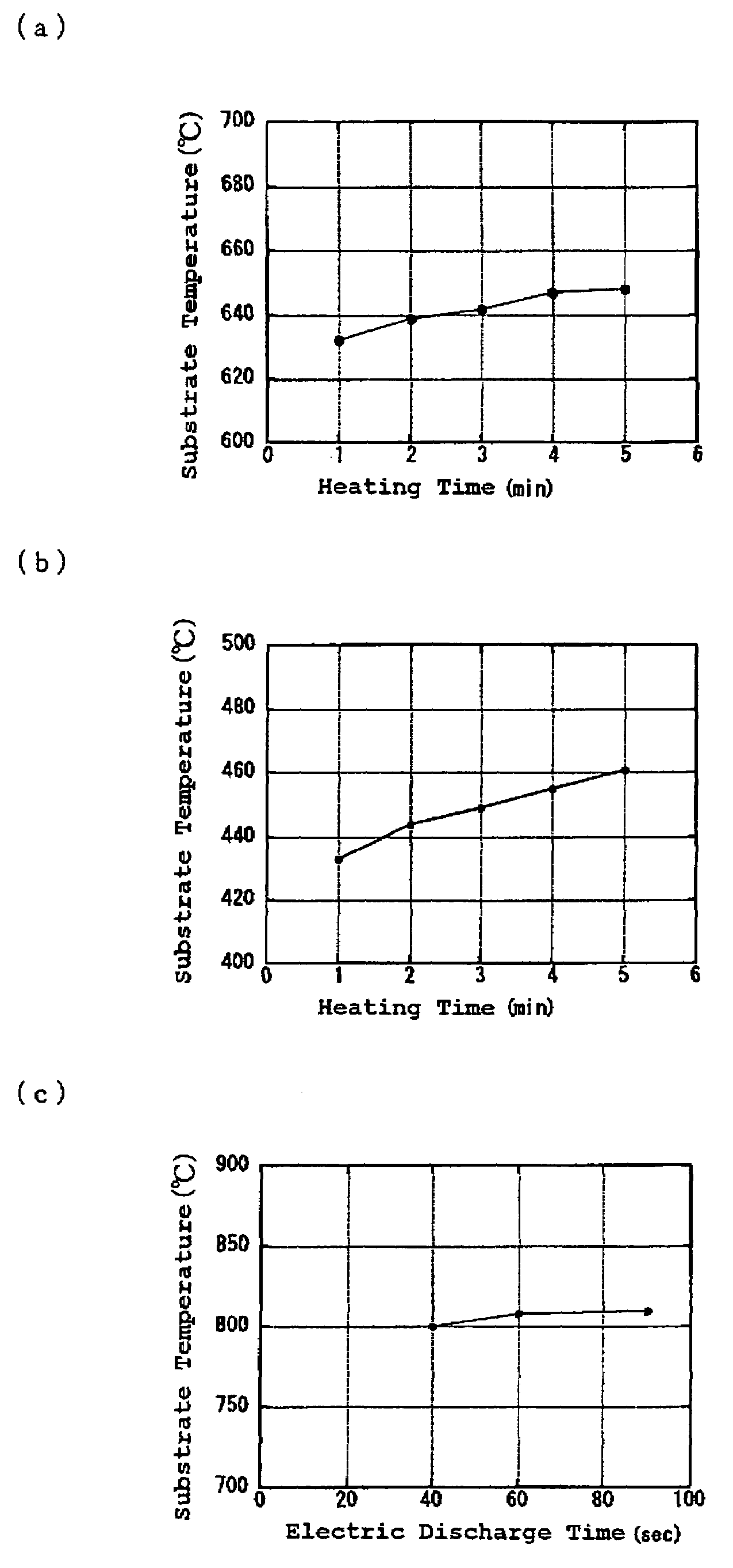
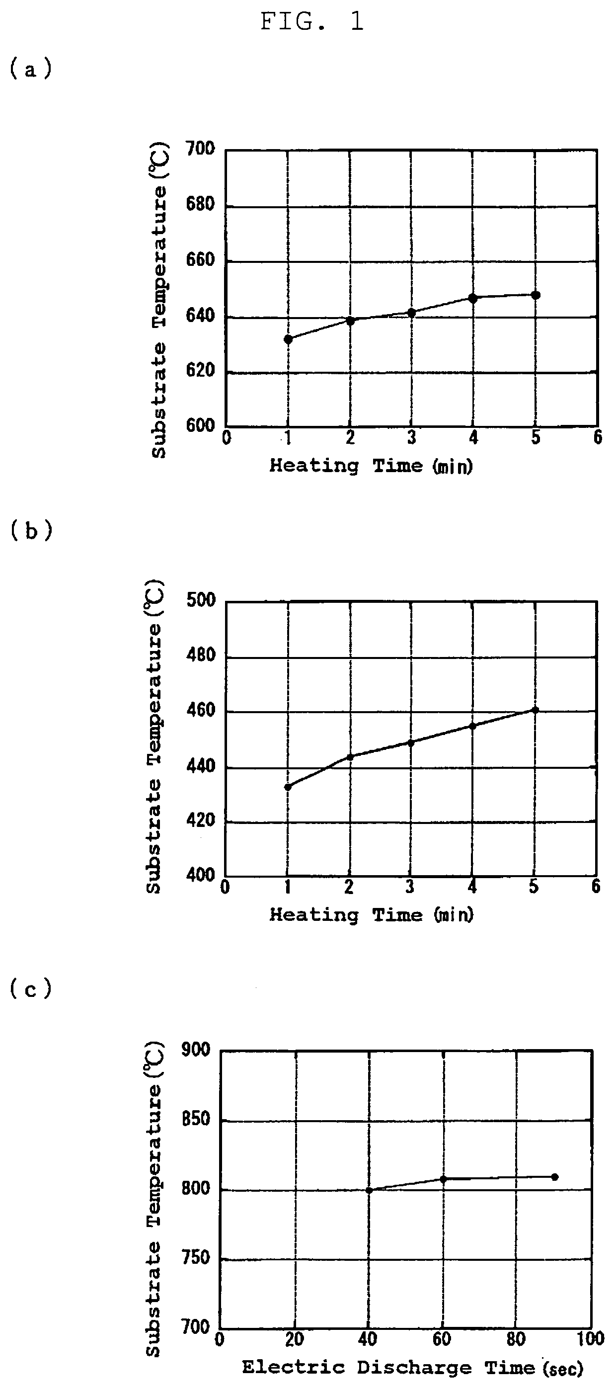
[0057]First, as the preparation before the bias treatment, the substrate was set on an electrode for applying a negative voltage (cathode), and vacuum evacuation was performed. Next, the substrate was heated (the first heating), and the temperature of the substrate was raised to 648° C. for 5 min (FIG. 1(a)). Next, a CH4 / H2 gas was introduced, and the base pressure was set to 115 Torr. Next, the substrate was heated again (the second heating), and the temperature of the substrate was raised to 461° C. for 5 min (FIG....


PUM


Abstract

There is disclosed a method for producing a substrate for single crystal diamond growth, comprising at least a step of preliminarily subjecting a substrate before single crystal diamond growth to a bias treatment for forming a diamond nucleus thereon by a direct-current discharge in which an electrode in a substrate side is a cathode, and wherein in the treatment, at least, a temperature of the substrate from 40 sec after an initiation of the bias treatment to an end of the bias treatment is held in a range of 800° C.±60° C. There can be provided a method for producing a substrate for single crystal diamond growth, by which a single crystal diamond can be grown more certainly.

Description

BACKGROUND OF THE INVENTION[0001]1. Field of the Invention[0002]The present invention relates to a method for producing a substrate for single crystal diamond growth.[0003]2. Description of the Related Art[0004]Diamond has a wide band gap of 5.47 eV and a very high dielectric breakdown electric field intensity of 10 MV / cm. Furthermore, it has the highest thermal conductivity in materials. Therefore, if this is used for an electronic device, the device is advantageous as a high output power device.[0005]On the other hand, diamond has high drift mobility and is the most advantageous as a high-speed power device in semiconductors in comparison of Johnson performance index.[0006]Accordingly, diamond is said to be the ultimate semiconductor suitable for high frequency / high power electronic devices.[0007]Therefore, a multilayer substrate in which a diamond film and the like is laminated on a substrate has attracted attention.[0008]Now, most of the single crystal diamonds for fabrication o...

Claims


Application Information

Patent Timeline
IPC IPC(8): C30B25/00C30B23/00C30B29/04
CPCC30B25/18C30B29/04H01L21/0242H01L21/02425H01L21/02658H01L21/02444H01L21/02491H01L21/02527H01L21/0262H01L21/02433
Inventor NOGUCHI, HITOSHI
Owner SHIN ETSU CHEM IND CO LTD
Learn More