Semiconductor light emitting element mounting member, and semiconductor light emitting device employing it

Inactive Publication Date: 2007-09-20
SUMITOMO ELECTRIC IND LTD
View PDF3 Cites 29 Cited by
  • Summary
  • Abstract
  • Description
  • Claims
  • Application Information

AI Technical Summary

Benefits of technology

[0021] As a result of the invention, the smoothness of the surface of the metal film can be improved.
[0022] More specifically, based on the shapes of the portions of the individual crystal grains of the metal or alloy forming the metal film exposed on the surface of the metal film, larger crystal grain particle diameters along the surface plane tend to increase unevenness of the surface. Also, the surface shape of the metal film is influenced by the surface shape of the underlying substrate, and greater surface roughness on the substrate tends to increase unevenness of the metal film surface. As the unevenness of the metal film surface increases, reflectivity decreases due to the tendency toward irregular reflection of light.
[0023] Accordingly, in one embodiment of the invention the individual crystal grains of the metal film have a particle diameter of no more than 0.5 μm along the plane of the metal film. This minimizes the unevenness of the metal film surface based on the shape of the portions exposed on the surface of the metal film. Also, by adjusting the substrate surface shape and the like to set the center-line average roughness Ra of the metal film surface to no more than 0.1 μm, the smoothness of the metal film surface can be improved and ligh

Problems solved by technology

While Ag, Al, and the like provide superior light reflectivity, the metal films actually formed on the element mounting surface, the reflective surface, or the like on the substrate do not provide adequate surface smoothness.
This results in the irregular reflection of light and prevents a high effective reflectivity from being obtained.
However, with thicker metal films there is a greater tendency

Method used


Image

  • Semiconductor light emitting element mounting member, and semiconductor light emitting device employing it
  • Semiconductor light emitting element mounting member, and semiconductor light emitting device employing it
  • Semiconductor light emitting element mounting member, and semiconductor light emitting device employing it

Examples


example

[0103] The present invention will be described below using examples and comparative examples.

first example

[0104] Twenty substrates with a length of 50.8 mm, a width of 50.8 mm, and a thickness of 0.3 mm made from aluminum nitride (AlN) having a thermal conductivity of 230 W / mK and a thermal expansion coefficient of 4.5×10⁶ / deg C were prepared. Lap abrasion and polishing were performed on both surfaces (main surfaces) of the substrates to apply a finish with a center-line average roughness Ra of 0.02 μm.

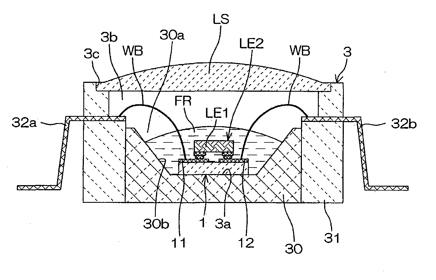
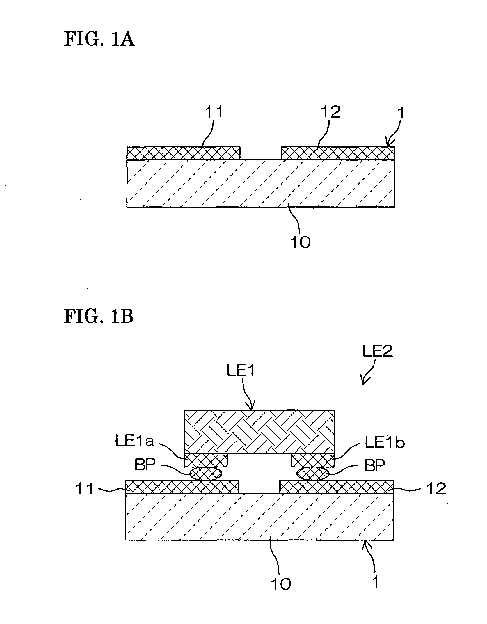
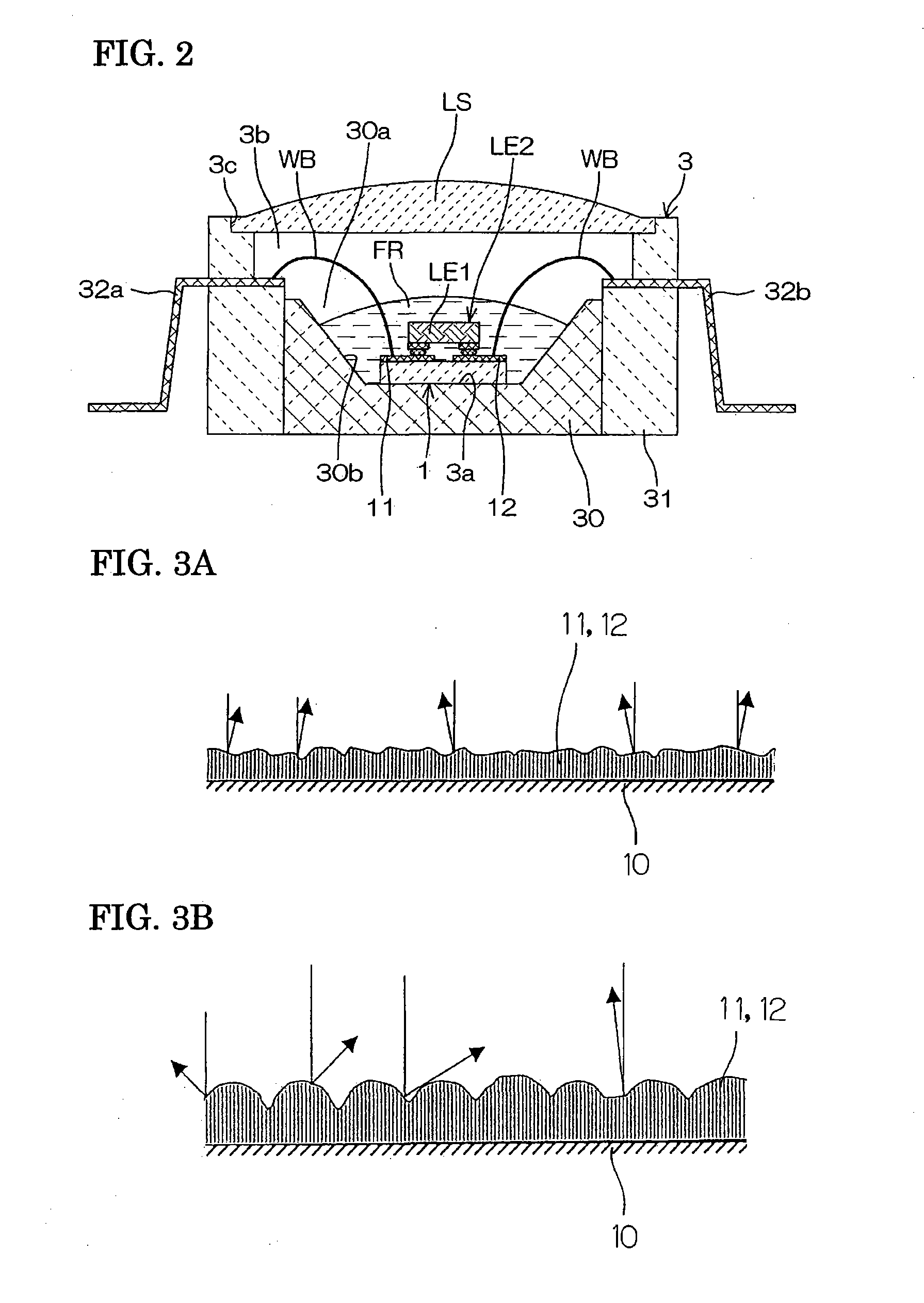
[0105] Next, as shown in FIG. 1A, vacuum vapor deposition was performed on a first main surfaces of the substrate 10 to form two pure aluminum films 11, 12 insulated from each other by a narrow gap on the planar center to form a submount 1 serving as the semiconductor light-emitting element mounting member. Film formation was performed as follows. First, on the first main surface of the substrates 10 were formed, in the same planar shape as the pure aluminum films 11, 12, a titanium adhesion layer having a thickness of 0.1 μm and a platinum barrier layer having a thickness of 0.2 μm, in ...

second example

[0108] Film-forming conditions were similar to those from the first example except that the substrate temperature was set to 80 deg C. On the first main surface of the aluminum nitride substrates 10 were formed a titanium adhesion layer having a thickness of 0.1 μm and a platinum barrier layer having a thickness of 0.2 μm. On top of this were formed the pure aluminum films 11, 12 having a thickness of 2 μm, to form the submount 1.

[0109] The mean particle diameter along the plane of the films of the aluminum crystal grains forming the pure aluminum films 11, 12 was determined using the method described above and was found to be 0.20 μm. Also, the mean value of the center-line average roughness Ra was calculated and found to be 0.042 μm. Also, light reflectivity was 88 percent, the die shear strength was 45 MPa, and the ball shear strength was 52 MPa.


PUM


Abstract

A semiconductor light-emitting element mounting member with an improved effective light reflectivity in a metal film serving as an electrode layer and/or a reflective layer, in which the metal layer has improved adhesion to a substrate, mechanical strength, and reliability and superior light-emitting characteristics. The semiconductor light-emitting element mounting member (a submount) is made by forming on a substrate metal films formed from Ag, Al, or an alloy containing these metals. The particle diameter of the crystal grains of the metal films is no more than 0.5 μm and the center-line average roughness Ra of the surface is no more than 0.1 μm. In a semiconductor light-emitting device, a semiconductor light-emitting element is mounted in the submount.

Description

CROSS-REFERENCE TO PRIOR APPLICATIONS [0001] This application is a U.S. national phase application under 35 U.S.C. §371 of International Patent Application No. PCT / JP2005 / 002758, filed Feb. 22, 2005, and claims the benefit of Japanese Application No. 2004-117, filed Apr. 12, 2004, both of which are incorporated by reference herein. The International Application was published in Japanese on Oct. 27, 2005 as International Publication No. WO 2005 / 101533 A1 under PCT Article 21(2).TECHNICAL FIELD [0002] The present invention relates to a semiconductor light-emitting element mounting member for mounting a semiconductor light-emitting element and a semiconductor light-emitting device with a semiconductor light-emitting element mounted in the semiconductor light-emitting element mounting member. BACKGROUND ART [0003] In order to improve the effective light-emission efficiency for semiconductor light-emitting devices, materials such as Ag and Al having superior light reflectivity are used t...

Claims


Application Information

Patent Timeline
IPC IPC(8): H01L31/12H01L33/56H01L33/58H01L33/60H01L33/62
CPCH01L33/60H01L2224/13H01L2224/48091H01L2224/48247H01L2224/45144H01L2924/00014H01L2924/00H01L2224/05573H01L2224/05568H01L2224/05599
Inventor AMOH, TERUOISHIDU, SADAMUHIGAKI, KENJIROTSUZUKI, YASUSHIFUKUDA, HIROSHI
Owner SUMITOMO ELECTRIC IND LTD
Why Eureka
Try Eureka