
Merged gate cascode transistor

a cascode transistor and merged gate technology, applied in the field of transistors, can solve the problems of large power and efficiency losses and excessive switching losses

Active Publication Date: 2007-09-20
INFINEON TECH AMERICAS CORP
View PDF6 Cites 84 Cited by
  • Summary
  • Abstract
  • Description
  • Claims
  • Application Information

AI Technical Summary

Benefits of technology

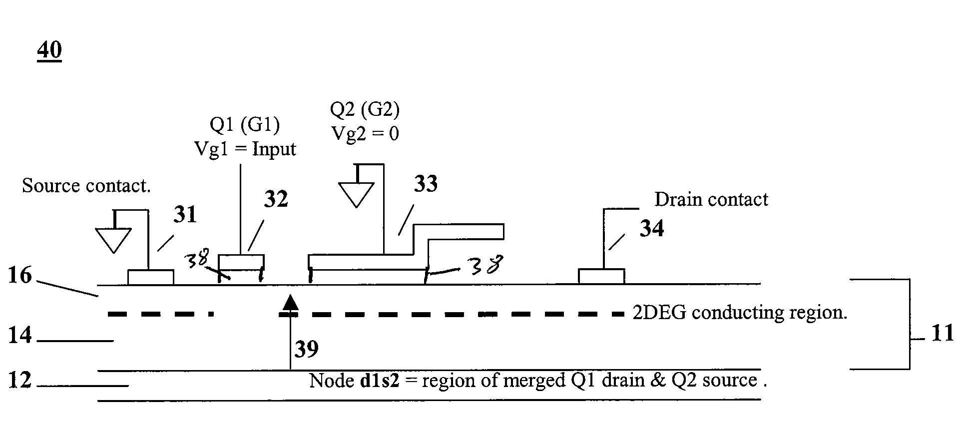
[0008]A merged cascode high electron mobility transistor in accordance with an embodiment of the present invention includes a first epitaxial layer of III-Nitride material, a second epitaxial layer of a III-Nitride material, positioned on top of said first epitaxial layer such that a 2 dimensional electron gas conducting layer is formed between the first and second epitaxial layers, a supply electrode electrically connected to the first epitaxial layer, a drain electrode electrically connected to the first epitaxial layer and spaced laterally from the supply electrode, a first gate positioned between the supply electrode and the drain electrode and capacitively coupled to the

Problems solved by technology

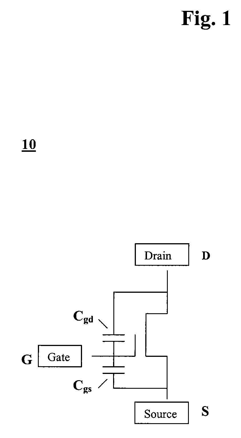
Large drain-source voltage (Vds) swings during switching create a large “Miller effect” and as a result, excessive switching losses.
This unwanted period of conduction may result in rather large power and efficiency losses.
These problems are common in all FET devices whether they are silicon, non-silicon or IEMT devices.

Method used


Image

  • Merged gate cascode transistor
  • Merged gate cascode transistor
  • Merged gate cascode transistor

Examples


Embodiment Construction

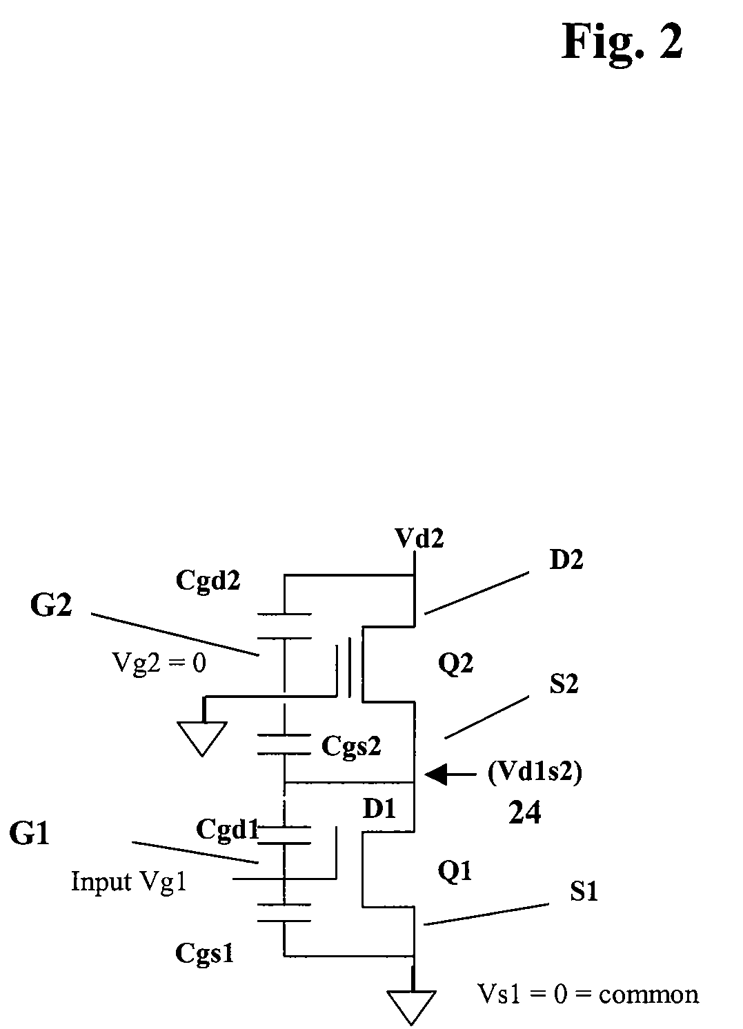
[0014]A transistor 20 suitable for use in high voltage, high speed switching applications in accordance with an embodiment of the present invention is described with reference to FIG. 2. A single FET 20 with two merged gates 22, 221 is illustrated in FIG. 2. That is, the FET 20 of FIG. 2 is a single device and not two separate FETs.

[0015]The top portion Q2 is in depletion mode, that is, normally ON with a depletion pinchoff voltage Vp2. The gate voltage Vg2 at the gate 221 of the top portion Q2 is set to 0, as illustrated. However, depending on the specific application, the gate voltage Vg2 may be set at any desired value.

[0016]The bottom portion Q1 of FET 20 is preferably in enhancement mode, that is, normally OFF, with an enhancement threshold voltage Vt1. An input voltage signal is preferably connected to the gate 22 to provide the gate voltage Vg1 at the gate 22 of the bottom portion Q1.

[0017]In operation, when the input voltage signal provides a high voltage at Vg1, the bottom ...


PUM


Abstract

A merged gate transistor in accordance with an embodiment of the present invention includes a semiconductor element, a supply electrode electrically connected to a top surface of the semiconductor element, drain electrode electrically connected to the top surface of the semiconductor element and spaced laterally away from the supply electrode, a first gate positioned between the supply electrode and the drain electrode and capacitively coupled to the semiconductor element to form a first portion of the transistor and a second gate positioned adjacent to the first gate, and between the supply electrode and the drain electrode to form a second portion of the transistor, wherein the second gate is also capacitively coupled to the semiconductor element. The first gate is connected to an input voltage signal such that conduction of the first portion is based on a value of the input voltage signal and the second gate is connected to a predetermined constant voltage such that the second portion of the transistor conducts until a voltage difference between the predetermined constant voltage and a voltage at the source electrode reaches a predetermined level.

Description

CROSS-REFERENCE TO RELATED APPLICATIONS[0001]The present application claims benefit of and priority to U.S. Provisional Application Ser. No. 60 / 783,934, filed on Mar. 20, 2006, entitled MERGED CASCODE TRANSISTOR (III-NITRIDE, COMPOUND, OR SILICON SEMICONDUCTOR) FOR LOW Qg, FAST SWITCHING AND HIGH VOLTAGE, the entire contents of which are hereby incorporated by reference herein.[0002]The present application is also related to U.S. patent application Ser. No. 11 / 345,753 entitled III-NITRIDE INTEGRATED SCHOTTKY AND POWER DEVICE filed Feb. 2, 2006, which claims benefit of and priority to U.S. Provisional Patent Application Ser. No. 60 / 649,393 entitled GaN MONOLITHIC FETKY SYNCHRONOUS RECTIFIER FOR BOOST DIODE filed Feb. 2, 2005, the entire contents of both of which are hereby incorporate by reference herein.BACKGROUND OF THE INVENTION[0003]The present invention relates to a transistor for use in high voltage, high speed switching applications. More specifically, the present application ...

Claims


Application Information

Patent Timeline
IPC IPC(8): H01L29/74
CPCH01L27/0605H01L27/0705H01L29/7787H01L29/42316H01L29/2003
Inventor HERMAN, THOMAS
Owner INFINEON TECH AMERICAS CORP
Learn More