Technique for isocentric ion beam scanning

a scanning and isocentric technology, applied in the field of semiconductor manufacturing, can solve the problems of beam-line variation, beam utilization and uniformity tuning, and unique challenges of low-energy ion beams, and achieve the effect of preventing charge buildup

Active Publication Date: 2007-09-27
VARIAN SEMICON EQUIP ASSOC INC
View PDF30 Cites 9 Cited by
  • Summary
  • Abstract
  • Description
  • Claims
  • Application Information

AI Technical Summary

Benefits of technology

[0019] In accordance with additional aspects of this particular exemplary embodiment, the method may further comprise preventing charge buildup on the wafer surface with a plasma flood gun that can be repositioned based on the predetermined angle of the ion beam.

Problems solved by technology

Compared with high- or medium-energy ion beams, low-energy ion beams present some unique challenges.
For example, a low-energy ion beam usually has a large beam spot, which can cause problems for beam utilization and uniformity tuning.
The problem of beam-line variation is not unique to low-energy ion beams but can also be observed in some high-current ion beams.
Such capabilities necessitate a sophisticated design of the end station 508 that is often expensive to build and maintain.

Method used


Image

  • Technique for isocentric ion beam scanning
  • Technique for isocentric ion beam scanning
  • Technique for isocentric ion beam scanning

Examples


Embodiment Construction

[0035] Embodiments of the present disclosure provide a new approach for isocentric ion beam scanning wherein an ion beam is tilted to a predetermined angle before the ion beam is directed into an end station for isocentric scanning of a target wafer. With the ion beam maintained at the predetermined angle, there may be no need to tilt the target wafer itself. As a result, isocentric scanning of the target wafer may involve a two-dimensional (2-D), rather than a three-dimensional (3-D), translation of the target wafer. Since it is no longer necessary to tilt the target wafer or to coordinate its 3-D movements, the end station may have a simpler and therefore less expensive design.

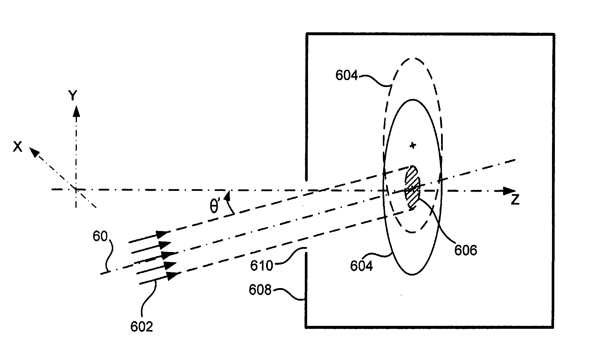
[0036]FIG. 6 illustrates an exemplary method for isocentric ion beam scanning in accordance with an embodiment of the present disclosure. In an ion implantation system, an end station 608 may hold a wafer 604. The normal direction of the wafer 604 may be aligned with the Z direction.

[0037] First, an ion be...


PUM


Abstract

A technique for isocentric ion beam scanning is disclosed. In one particular exemplary embodiment, the technique may be realized by an apparatus for isocentric ion beam scanning. The apparatus may comprise an end station having a mechanism for holding and translating a wafer. The apparatus may also comprise a deflector that tilts an ion beam to a predetermined angle and directs the ion beam into the end station. The wafer may be translated with respect to the ion beam for isocentric scanning at least a portion of a surface of the wafer, and wherein the ion beam is maintained at the predetermined angle during isocentric scanning.

Description

FIELD OF THE DISCLOSURE [0001] The present disclosure relates generally to semiconductor manufacturing and, more particularly, to a technique for isocentric ion beam scanning. BACKGROUND OF THE DISCLOSURE [0002] Ion implantation is a process of depositing chemical species into a substrate by direct bombardment of the substrate with energized ions. In semiconductor manufacturing, ion implanters are used primarily for doping processes that alter the type and level of conductivity of target materials. A precise doping profile in an integrated circuit (IC) substrate and its thin-film structure is often crucial for proper IC performance. To achieve a desired doping profile, one or more ion species may be implanted in different doses, at different energy levels, and sometimes at different incident angles. [0003] For a uniform distribution of dopant ions, an ion beam is typically scanned across the surface of a target wafer. FIG. 1a shows a typical beam path 10 formed by scanning an ion be...

Claims


Application Information

Patent Timeline
Patent Type & Authority Applications(United States)
IPC IPC(8): H01J37/317
CPCH01J37/3023H01J37/3171H01J2237/30483H01J2237/20228H01J2237/0458
Inventor OLSON, JOSEPH C.RENAU, ANTHONY
Owner VARIAN SEMICON EQUIP ASSOC INC
Why Eureka
Try Eureka