Wavelength converting devices

a conversion device and wavelength technology, applied in the direction of instruments, light demodulation, optical waveguide light guides, etc., can solve the problems of limiting the resistance of material forming periodic polarization inversion structures to resist optical damage, unable to oscillate converted light of a high output power of, for example, 1 w or more, and unable to achieve high output power. , to achieve the effect of limiting the conversion efficiency of fundamental light to harmonic wave, and reducing the output power ratio ratio

Active Publication Date: 2007-09-27
NGK INSULATORS LTD
View PDF9 Cites 17 Cited by
  • Summary
  • Abstract
  • Description
  • Claims
  • Application Information

AI Technical Summary

Benefits of technology

[0011] The prevent inventors have reached the idea of forming a pair of thinner portions in a substrate of a bulk-shaped electro-optical material and of forming a wavelength converting portion having a cross sectional area of 0.0001 mm2 or larger and 0.01 mm2 or smaller between them. The cross sectional area of 0.0001 mm2 corresponds with 100 μm2 (length of 10 μm and width of 10 μm). The converting portion defined by this area does not generally have a function of a channel optical waveguide and single mode propagation. However, in the case that a periodic domain inversion structure is formed in the converting portion, a higher output power can be obtain

Problems solved by technology

However, according to prior SHG devices, the material forming the periodic polarization inversion structure has the limit on the resistance against optical damage.
It is proved to be difficult to oscillate converted light of a high output power of, for example, 1 W or more.
However, for example as an SHG output power of 200 mW or more, optical damage may be

Method used


Image

  • Wavelength converting devices
  • Wavelength converting devices
  • Wavelength converting devices

Examples


example 1

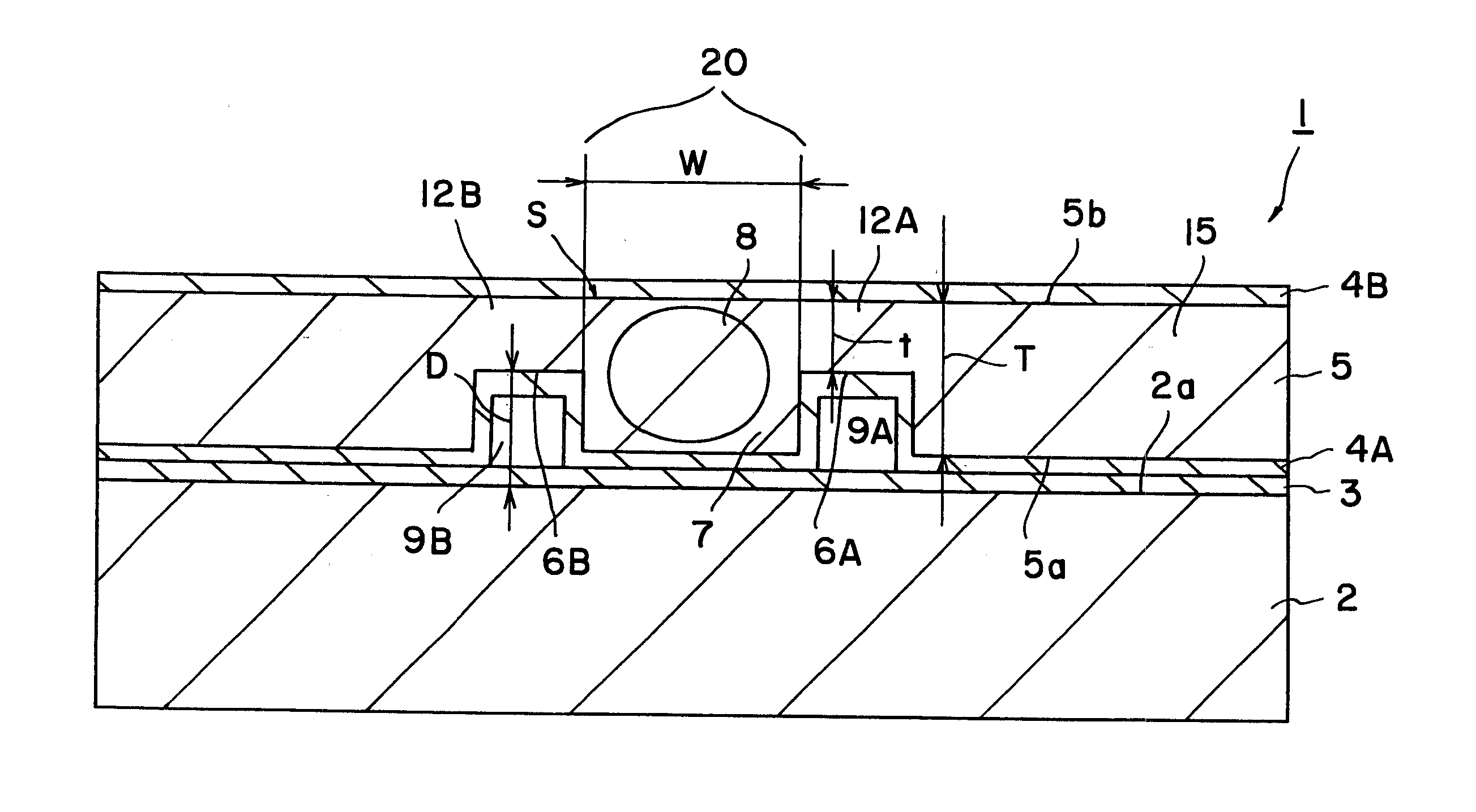
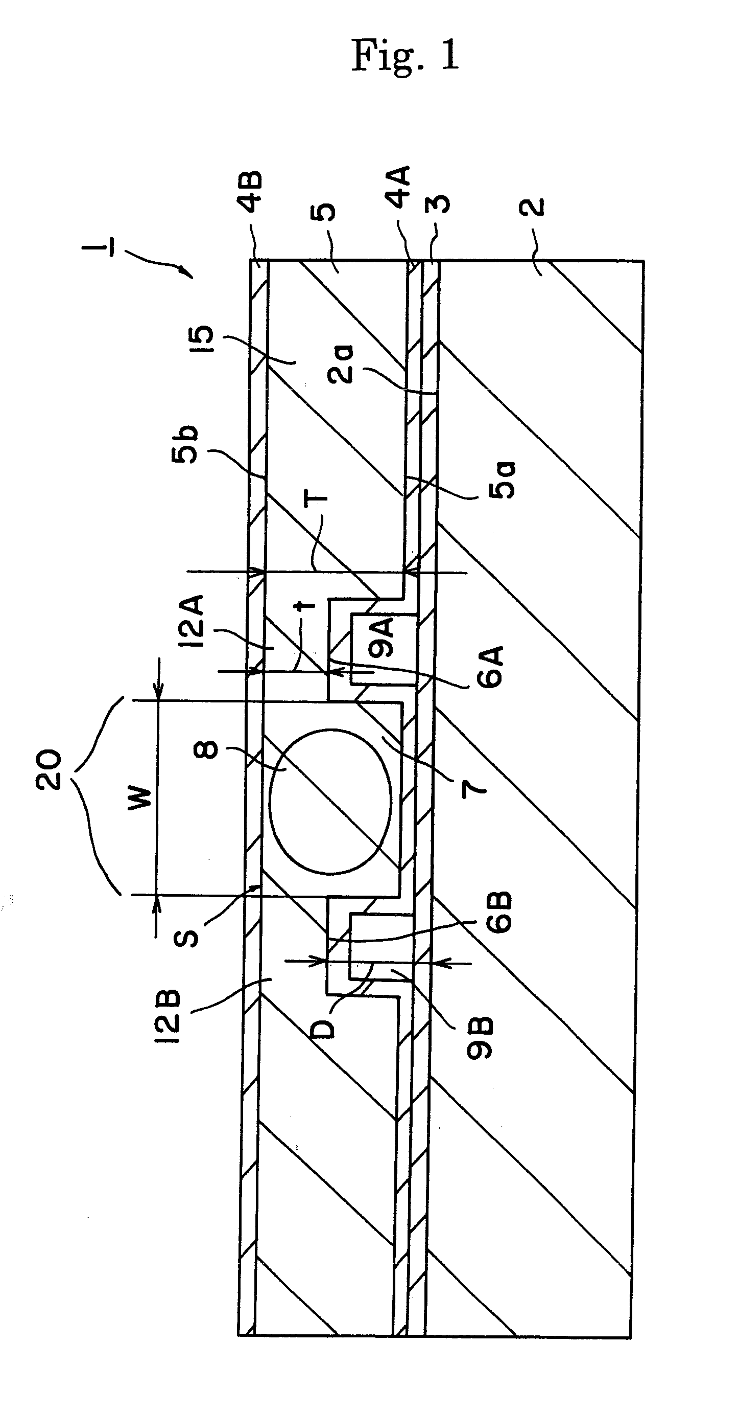
[0059] The device 1 described referring to FIG. 1 was produced.

[0060] Specifically, periodic polarization domain inversion structure having a period of 6.54 μm was produced in a Z-cut substrate having a thickness of 500 μm and made of MgO-doped lithium niobate. SiO2 film having a thickness of 0.5 μm was formed thereon by sputtering. Further, Mo film of a thickness of 0.5 μg / m was formed by sputtering and then patterned to produce an etching mask. Wet etching was then performed in a fluoric acid solution heated at 60° C. to form the grooves 6A and 6B. The depth “D” of the groove was 20 μm and the distance between the grooves was 50 μm.

[0061] An adhesive was applied on the substrate 2 having a thickness of 1 mm and made of non-doped lithium niobate. The substrate 2 was then adhered to the above substrate 5 of MgO-doped lithium niobate. The surface 5b of the substrate 5 of MgO-doped lithium niobate was removed by grinding and polishing to a thickness of 50 μm. SiO2 film 4B having a t...

example 2

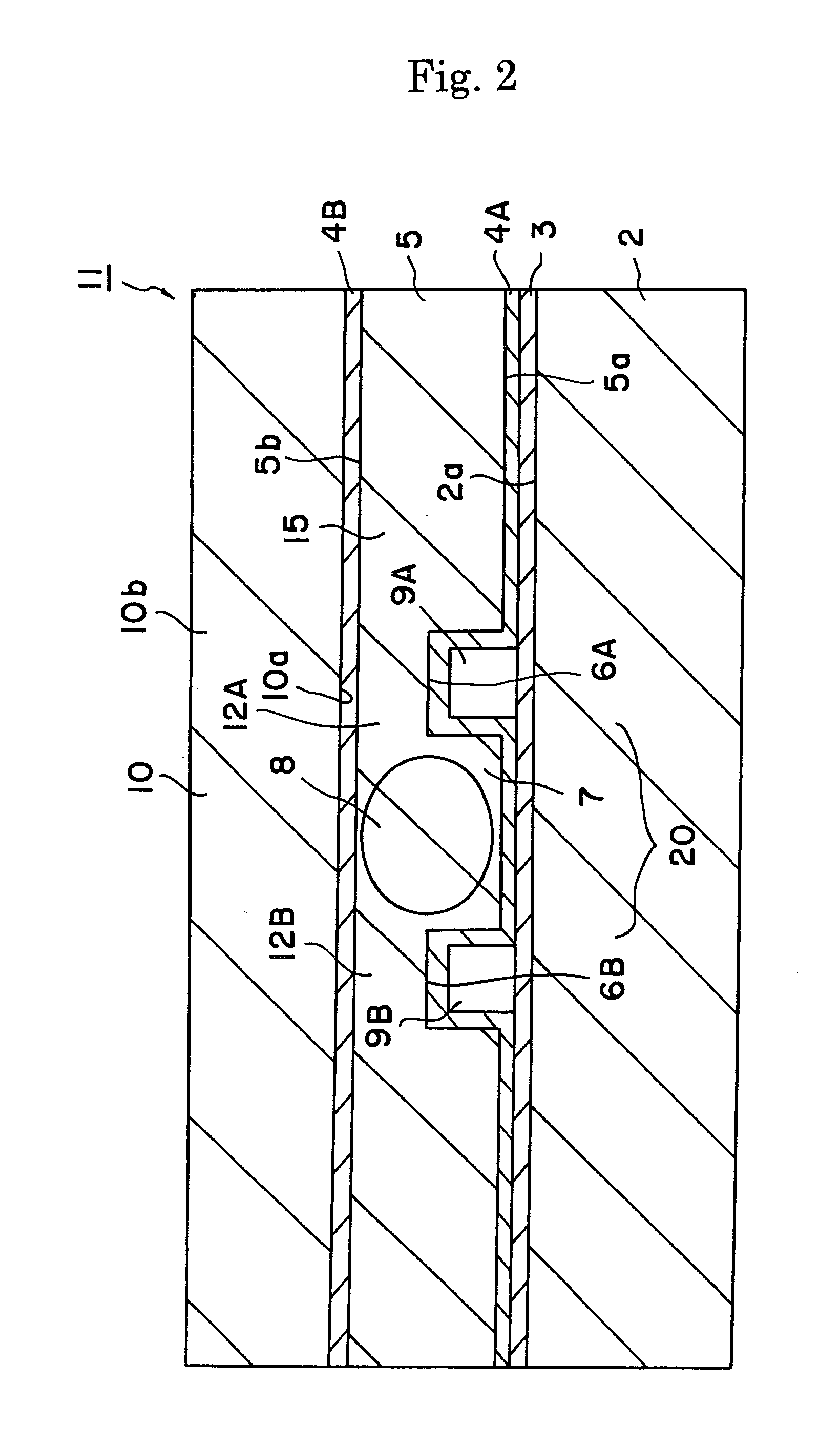
[0063] The device 1 described referring to FIG. 1 was produced.

[0064] Periodic polarization domain inversion structure having a period of 6.54 μm was produced in a Z-cut substrate having a thickness of 500 μm and made of MgO-doped lithium niobate. SiO2 film having a thickness of 0.5 μm was formed by sputtering. Further, Mo film of a thickness of 0.5 μm was formed by sputtering and then patterned to produce an etching mask. Wet etching was then performed in a fluoric acid solution heated at 60° C. to form the grooves 6A and 6B. The depth “D” of the groove was 5 μm and the distance between the grooves was 100 μm.

[0065] An adhesive was applied on the substrate 2 having a thickness of 1 mm and made of non-doped lithium niobate. The substrate 2 was then adhered to the above substrate 5 of MgO-doped lithium niobate. The surface 5b of the substrate 5 of MgO-doped lithium niobate was removed by grinding and polishing to a thickness of 10, m. Ta2O5 film 4B having a thickness of 0.5 μm was ...


PUM


Abstract

A wavelength converting device 1 has a substrate 5 made of an electro-optic material and converts a wavelength of a fundamental light to oscillate a converted light. A wavelength converting portion 7 is provided in the substrate 5 and has a cross sectional area of 0.0001 mm2 or larger and 0.01 mm2 or smaller. A pair of thinner portions 12A and 12B are provided in both sides of the wavelength converting portion, respectively, and thinner than the wavelength converting portion 7.

Description

BACKGROUND OF THE INVENTION [0001] 1. Field of the Invention [0002] The invention relates to a wavelength converting device such as an SHG device. [0003] 2. Related Arts [0004] Non-linear optical crystals, such as lithium niobate or lithium tantalite, have a high second-order non-linear optical constant. It is thus possible to realize a quasi-phase matched (QPM) type second harmonic generation (SHG) device, by providing a periodic polarization domain inversion structure in the crystal. Further, an SHG device of a high efficiency can be realized by forming a waveguide in the periodic polarization domain inversion structure, and the device finds a wide variety of applications such as optical communication, medical uses, optochemical uses, various optical measurements, etc. [0005] The applicant disclosed a process of producing a ridge-shaped optical waveguide used for a device for generating second harmonic wave, in Japanese Patent publication H09-269430A. The waveguide is formed by su...

Claims


Application Information

Patent Timeline
IPC IPC(8): G02F1/35G02F2/02
CPCG02F1/353G02F2202/20G02F2001/3548G02F1/3551G02F1/3548
Inventor YOSHINO, TAKASHIYAMAGUCHI, SHOICHIRO
Owner NGK INSULATORS LTD
Why Eureka
Try Eureka