Semiconductor device

a technology of semiconductors and devices, applied in the direction of burglar alarm mechanical actuation, burglar alarm by hand-portable articles removal, instruments, etc., can solve the problems of inability to generate the power required for transmitting and receiving individual information, difficult to transmit and receive signals from a long distance, etc., to prevent power shortages for transmitting and extend the communication distance between a reader/writer and the rfid.

Active Publication Date: 2007-10-04
SEMICON ENERGY LAB CO LTD
View PDF27 Cites 122 Cited by
  • Summary
  • Abstract
  • Description
  • Claims
  • Application Information

AI Technical Summary

Benefits of technology

[0023] The semiconductor device of the present invention includes a battery. Therefore, similarly to a conventional semiconductor device, the semiconductor device of the present invention can prevent power shortage for transmitting and receiving individual information associated with deterioration over time of a cell. In addition, the semiconductor device of the present invention has an antenna which receives a signal for supplying power to the battery. Therefore, when power of radio waves from outside is used, the battery can be charged without direct connection between the semiconductor device and a charger. Accordingly, the semiconductor device of the present invention can be continuously used without generating confirmation of remaining capacity of a cell and replacement of a cell, like an active type RFID. In addition, power for driving the RFID is always held in the battery, so that enough power for operating the RFID can be obtained and a communication distance between a reader / writer and the RFID can be extended.

Problems solved by technology

However, as shown in FIG. 31, in the case of a semiconductor device which has an active type RFID provided with a cell for driving, there has been a problem in that the cell consumes over time, and eventually power required for transmitting and receiving individual information cannot be generated in accordance with transmission and reception of individual information and setting of the intensity of radio waves required for transmission and reception.
Accordingly, there has been a problem in that confirmation of remaining capacity of a cell and replacement of a cell are generated in order to continuously use a semiconductor device which has an active type RFID provided with a cell for driving.
In addition, as shown in FIG. 32, in the case of a semiconductor device having a passive type RFID which generates a power supply for driving by using power of radio waves (carrier waves) from outside, there has been a problem in that it is difficult to transmit and receive signals from a long distance and to secure power for transmitting radio waves required for transmission and reception, so that it is difficult to realize transmission and reception in excellent condition.
Accordingly, there has been a problem in that a distance from an antenna of a reader / writer which is a power supply means to which enough power of radio waves (carrier waves) from outside is supplied is limited to be short, in order to use a semiconductor device having a passive type RFID which generates a power supply for driving by using power of radio waves (carrier waves) from outside.

Method used


Image

  • Semiconductor device
  • Semiconductor device
  • Semiconductor device

Examples


embodiment mode 1

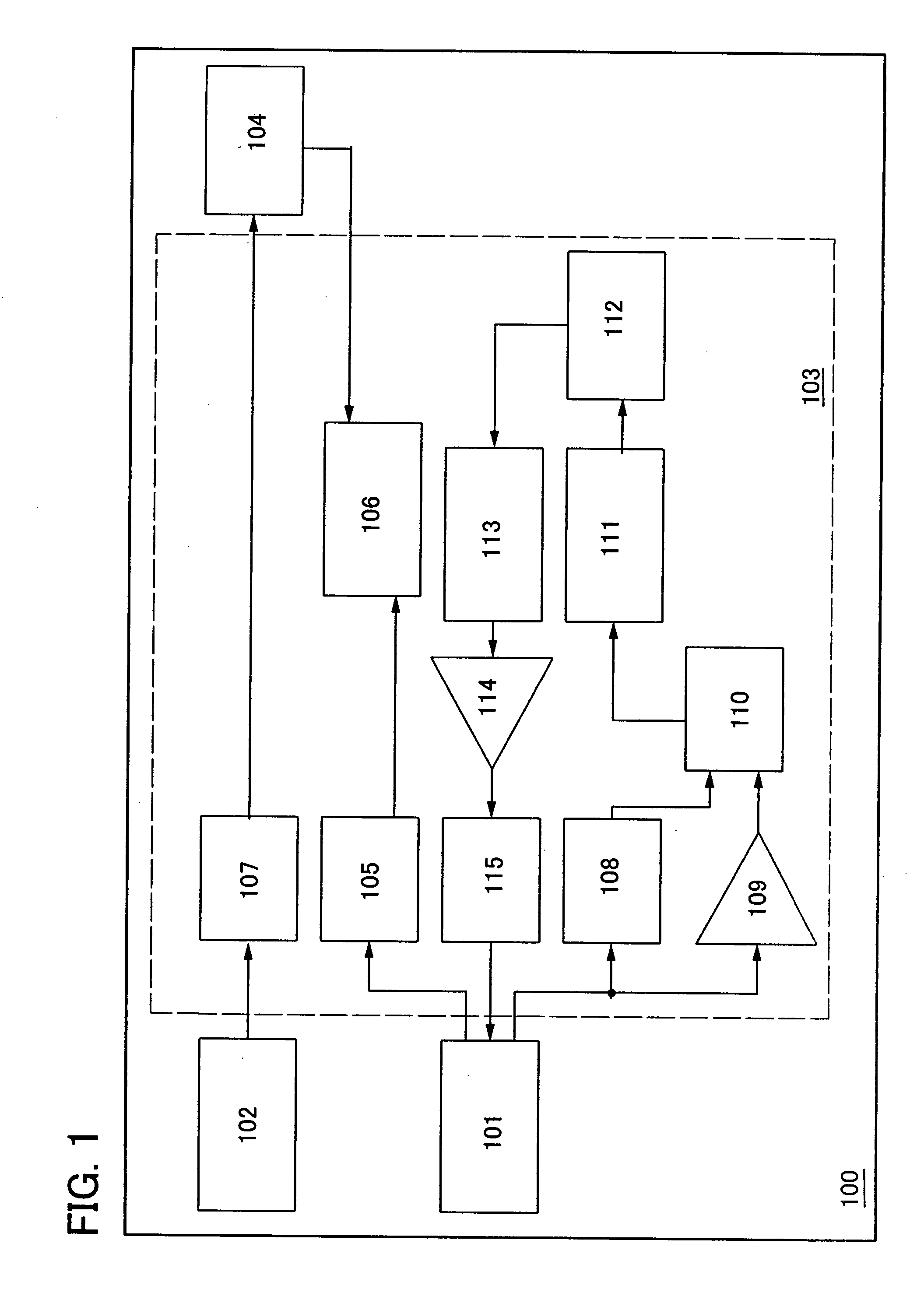
[0058] A semiconductor device used for an RFID of the present invention will be described with reference to block diagrams shown in FIGS. 1 and 2.

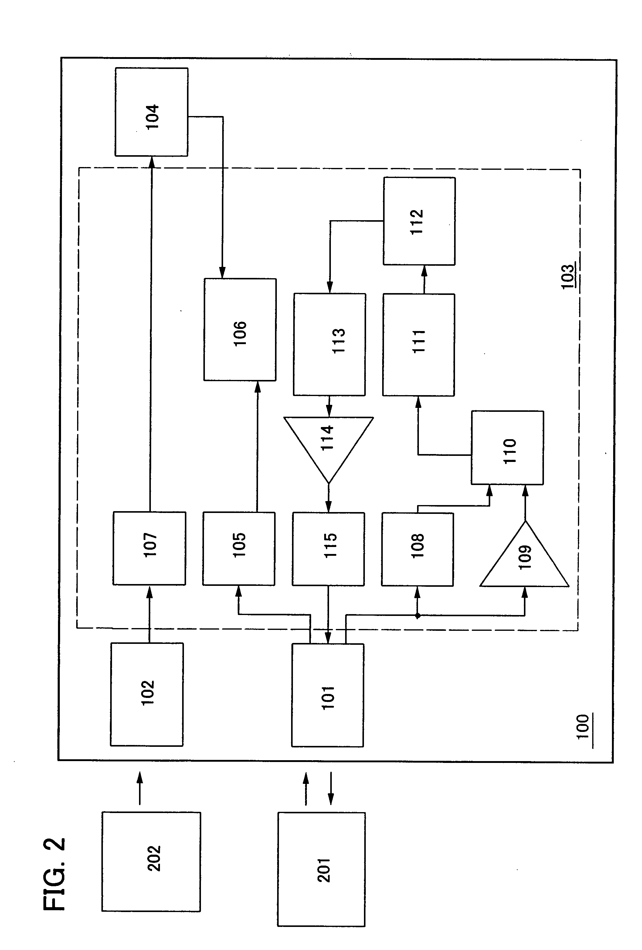
[0059] An RFID 100 of FIG. 1 includes a first antenna circuit 101, a second antenna circuit 102, a signal processing circuit 103, and a battery 104. The signal processing circuit 103 includes a first rectifier circuit 105, a power supply circuit 106, a second rectifier circuit 107, a demodulation circuit 108, an amplifier 109, a logic circuit 110, a memory control circuit 111, a memory circuit 112, a logic circuit 113, an amplifier 114, and a modulation circuit 115.

[0060] In addition, FIG. 2 shows a block diagram in which the first antenna circuit 101 transmits and receives a signal to and from a reader / writer 201, and the second antenna circuit 102 receives a signal from a charger 202. In FIG. 2, the signal received by the first antenna circuit 101 is inputted to the power supply circuit 106 through the first rectifier circuit 105. In F...

embodiment mode 2

[0088] This embodiment mode will describe a structure having a booster antenna circuit (hereinafter referred to as a booster antenna) in a semiconductor device having the RFID shown in Embodiment Mode 1, with reference to drawings. Note that in the drawings which are used in this embodiment mode, the same reference numerals are used for the same portions as in Embodiment Mode 1.

[0089] Note that a booster antenna described in this embodiment mode means an antenna (hereinafter referred to as a booster antenna) which is larger than an antenna (hereinafter referred to as a first chip antenna or a first antenna circuit) which receives a signal from a reader / writer and outputs it to a signal processing circuit of an RFID included in a semiconductor device, or an antenna (hereinafter referred to as a second chip antenna or a second antenna circuit) which receives a signal from a charger included in the semiconductor device. The booster antenna and the first chip antenna or the second chip...

embodiment mode 3

[0117] This embodiment mode will describe an example of a method for manufacturing the semiconductor device shown in the above embodiment modes, with reference to drawings.

[0118] First, a release layer 1903 is formed over one surface of a substrate 1901 with an insulating film 1902 interposed therebetween, and sequentially, an insulating film 1904 which serves as a base film and a semiconductor film 1905 (a film containing amorphous silicon, for example) are stacked in FIG. 19A. Note that the insulating film 1902, the release layer 1903, the insulating film 1904, and the semiconductor film 1905 can be formed sequentially.

[0119] Note that as the substrate 1901, a glass substrate, a quartz substrate, a metal substrate (such as a ceramic substrate or a stainless steel substrate), or a semiconductor substrate such as a Si substrate can be used. In addition, as a plastic substrate, a substrate formed of polyethylene terephthalate (PET), polyethylene naphthalate (PEN), polyether sulfone...


PUM


Abstract

The present invention provides a battery as a power supply for supplying power in the RFID, and another antenna for charging the battery, in addition to an antenna which transmits and receives individual information to and from outside as a means for supplying power to the battery.

Description

TECHNICAL FIELD [0001] The present invention relates to a semiconductor device. In particular, the present invention relates to a semiconductor device which transmits and receives data through radio waves and receives power. Furthermore, the present invention relates to a communication system using a semiconductor device through radio waves, an antenna and a reader / writer which transmit and receive data to and from the semiconductor device, and an antenna and a charger which supply power to the semiconductor device. [0002] Note that a semiconductor device in this specification refers to all devices which can function by using a semiconductor property. BACKGROUND ART [0003] In recent years, an individual identification technique using radio waves such as electromagnetic waves for wireless communication has attracted attention. In particular, as a semiconductor device which communicates data by wireless communication, an individual identification technique using an RFID (Radio Frequen...

Claims


Application Information

Patent Timeline
Patent Type & Authority Applications(United States)
IPC IPC(8): G08B13/14G06K19/07H01L21/822H01L27/04
CPCG06K19/0701G06K19/0702H01Q1/2225G06K19/07767G06K19/0723G06K19/077H01L21/822H01Q7/00
Inventor YAMAZAKI, SHUNPEIKOYAMA, JUNISHII, MASATOATSUMI, TOMOAKIOSADA, TAKESHIIKEDA, TAKAYUKIKUROKAWA, YOSHIYUKISHIONOIRI, YUTAKA
Owner SEMICON ENERGY LAB CO LTD
Why Eureka
Try Eureka