High-voltage tolerant power-rail ESD clamp circuit

Active Publication Date: 2007-10-04
NATIONAL CHIAO TUNG UNIVERSITY
View PDF10 Cites 26 Cited by
  • Summary
  • Abstract
  • Description
  • Claims
  • Application Information

AI Technical Summary

Benefits of technology

[0008] An object of the present invention is to provide a high-voltage tolerant power-rail ESD clamp circuit, in which an ESD detection circuit is used to provide a substrate-triggered current to an ESD protection element when an ESD event occurs so as to enhance the turn-on speed and turn-on uniformity.
[0009] Another object of the present invention is to provide a high-voltage tolerant power-rail ESD clamp circuit, in which the ESD detection circuit can match different ESD protection elements for use to meet different applications or specifications.
[0010] Another object of the present invention is to provide a high-voltage tolerant power-rail ESD clamp circuit, in which there won't be any gate-oxide reliability issue when applying the ESD detection circuit to mixed-voltage IO interfaces.
[0011] To achieve the above objects, the present invention provides a high-voltage tolerant power-rail ESD clamp circuit, which comprises an ESD detection circuit and an ESD protection element. The ESD detection circuit is connected to at least a voltage source and a ground terminal and used to detect whether there is ESD between the voltage source and the ground terminal. The ESD detection circuit further comprises a voltage divider for splitting an input voltage of the voltage source into two divided voltages, a substrate driver for driving a substrate to produce a trigger current, an RC distinguisher, a fourth transistor and a second resistor. The ESD protection element is triggered on via the trigger current of the trigger node by the ESD detection circuit to quickly and uniformly discharge an ESD current in an ESD situation, hence having no gate-oxide reliability issue.

Problems solved by technology

Though ICs with mixed-voltage circuits can be manufactured with both thin and thick gate-oxide devices by using extra process steps and additional mask layers, but they will increase the product cost and lower the production yield.
Moreover, a thick-gate-oxide device has inferior device characteristics than that of the thin one, so that the operating frequency of chips will be limited.
But if this kind of device is used alone as the ESD protection element, the turn-on speed will be slower and the turn-on voltage will be higher during ESD, hence being unable to effectively protect internal circuits with thin gate oxides.
If a forward-biased diode string is used as the ESD protection element, although a faster turn-on speed can be achieved, there will be a very large leakage current during operation under high temperatures because of parasitic pnp BJTs and Darlington beta gain.
But this kind of devices can only tolerate a maximum power supply voltage, no more than two times of their device limitation.
If the power supply voltage exceeds two times of their device limitation, the gate-oxide reliability issue of device will arise.
In order to acquire a better ESD protection capability, a larger chip area is required, and different ESD elements cannot be matched for use, hence being less flexible.
Although other ESD protection elements without gate oxide such as silicon-controlled rectifiers (SCRs) can operate under high power supply voltages without oxide gate reliability issue, these elements usually have a very slow turn-on speed and a too high turn-on voltage, and cannot effectively protect the chip circuits when used alone without being triggered by external circuits.
Moreover, existing trigger circuits cannot operate under a power supply voltage three times of their device limitation.

Method used


Image

  • High-voltage tolerant power-rail ESD clamp circuit
  • High-voltage tolerant power-rail ESD clamp circuit
  • High-voltage tolerant power-rail ESD clamp circuit

Examples


Embodiment Construction

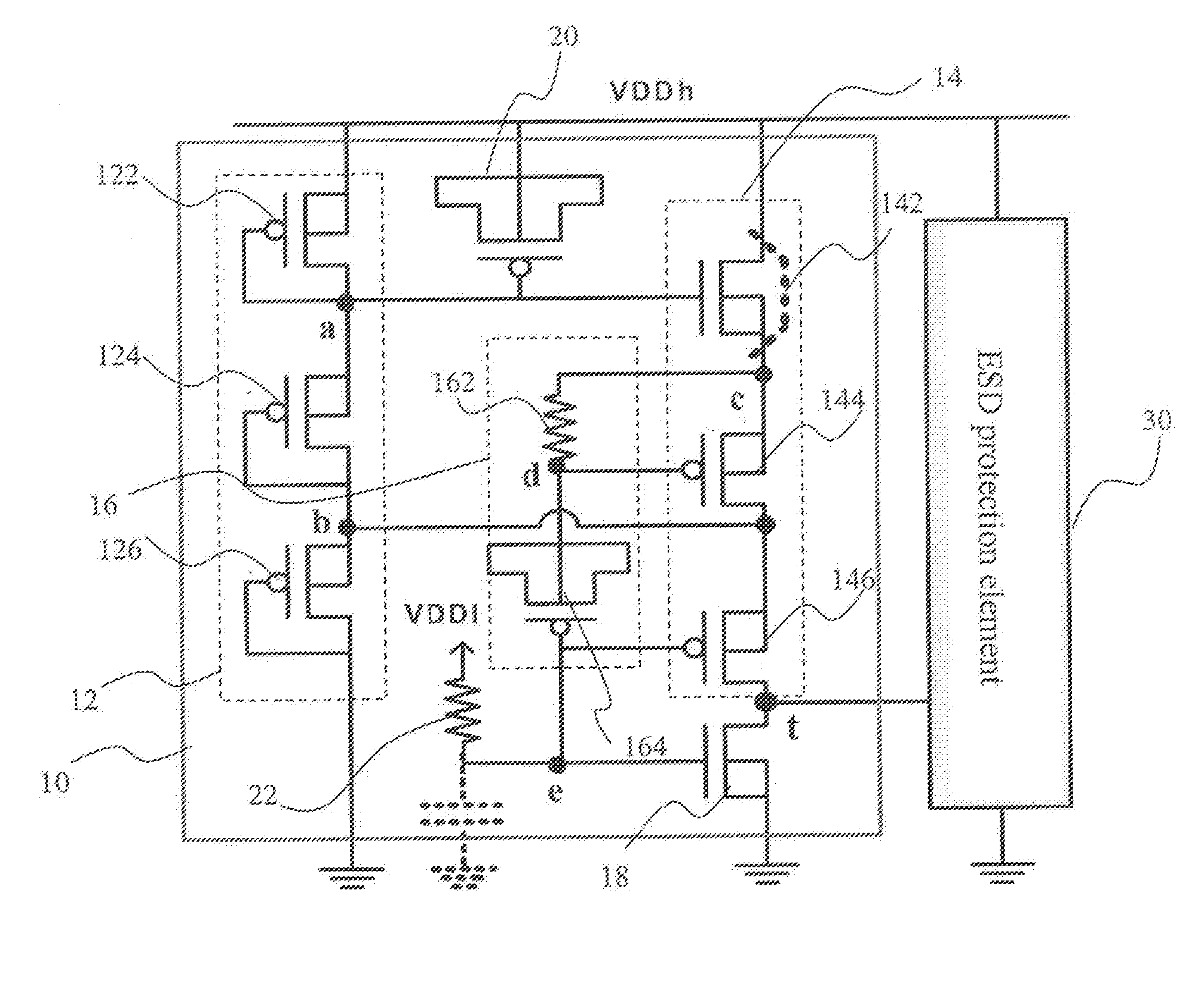
[0019] The present invention provides a high-voltage tolerant power-rail ESD clamp circuit, in which a substrate-triggered current is provided to drive different ESD protection elements under ESD stress. The substrate-triggered current has been reported to be beneficial to many ESD protection devices, such as the STNMOS (substrate-triggered NMOS) device, the SCR device, and the FOD (field oxide) device. The substrate-triggered current can improve ESD robustness of these ESD protection devices by increasing their turn-on speed and turn-on uniformity under ESD stress.

[0020] As shown in FIG. 1, a power-rail ESD clamp circuit of the present invention comprises two voltage sources VDDh and VDDl, an ESD detection circuit 10 and an ESD protection element 30. The ESD detection circuit 10 is composed of a voltage divider 12, a substrate driver 14, an RC distinguisher 16, a fourth transistor 18, a fifth transistor 20 and a second resistor 22. The voltage divider 12 includes three p-type tran...


PUM


Abstract

A high-voltage tolerant power-rail ESD clamp circuit is proposed, in which circuit devices can safely operate under the high power supply voltage that is three times larger than their process limitation without gate-oxide reliability issue. Moreover, an ESD detection circuit is used to effectively improve the whole ESD protection function by substrate-triggered technique. Because only low voltage (1*VDD) devices are used to achieve the object of high voltage (3*VDD) tolerance, the proposed design provides a cost effective power-rail ESD protection solution to chips with mixed-voltage interfaces.

Description

BACKGROUND OF THE INVENTION [0001] 1. Field of the Invention [0002] The present invention relates to an ESD clamp circuit and, more particularly, to a high-voltage tolerant power-rail ESD clamp circuit. [0003] 2. Description of Related Art [0004] ESD protection is used to protect ICs from damage due to ESD events. When applied to a mixed-voltage IO interface, because there simultaneously exists more than two power supply voltages on this interface, both thin and thick gate oxide devices are usually simultaneously used with the considerations on product reliability, operating frequency, chip area, and so on. Though ICs with mixed-voltage circuits can be manufactured with both thin and thick gate-oxide devices by using extra process steps and additional mask layers, but they will increase the product cost and lower the production yield. Moreover, a thick-gate-oxide device has inferior device characteristics than that of the thin one, so that the operating frequency of chips will be li...

Claims


Application Information

Patent Timeline
IPC IPC(8): H02H9/00
CPCH01L27/0285H02H3/22
Inventor KER, MING-DOUCHEN, WEN-YI
Owner NATIONAL CHIAO TUNG UNIVERSITY
Why Eureka
Try Eureka