Semiconductor Device

a technology of semiconductor devices and bumps, which is applied in the direction of electrical apparatus construction details, manufacturing tools, basic electric elements, etc., can solve the problems of slow electric resistivity and unsuitable high-speed devices, and achieve the effect of improving the reliability of the semiconductor device and increasing the strength of connection between the connection electrode and the bump

Active Publication Date: 2007-10-04
ROHM CO LTD
View PDF7 Cites 35 Cited by
  • Summary
  • Abstract
  • Description
  • Claims
  • Application Information

AI Technical Summary

Benefits of technology

[0013] However, the invention defines that with respect to the opposing direction of the functional surface and the connection surface, the sum of the height of the connection electrode and the height of the bump is not less than a half of the predetermined distance between the functional surface and the connection surface, whereby the connecting member formed of the material having the high electrical resistivity can be decreased in length (thickness). Accordingly, the electrical resistance between the solid device and the semiconductor chip can be reduced. As a result, the semiconductor device is suitable for use in the high-speed devices.
[0032] On the other hand, the connection portion (connecting member) between the bump and the connection electrode (the bump of the another semiconductor chip) is shifted (offset) toward the solid device or the semiconductor chip from the position where the stress exerted on the conductive member peaks (the intermediate portion between the mutually opposing functional surface and connection surface). Therefore, if such an underfill layer is provided, the heat cycling is less likely to cause the rupture at the connection portion between the bump and the connection electrode.

Problems solved by technology

The semiconductor device 51 having such a great electrical resistivity operates so slow that it is not suited for use in high-speed devices.

Method used


Image

  • Semiconductor Device
  • Semiconductor Device
  • Semiconductor Device

Examples


first embodiment

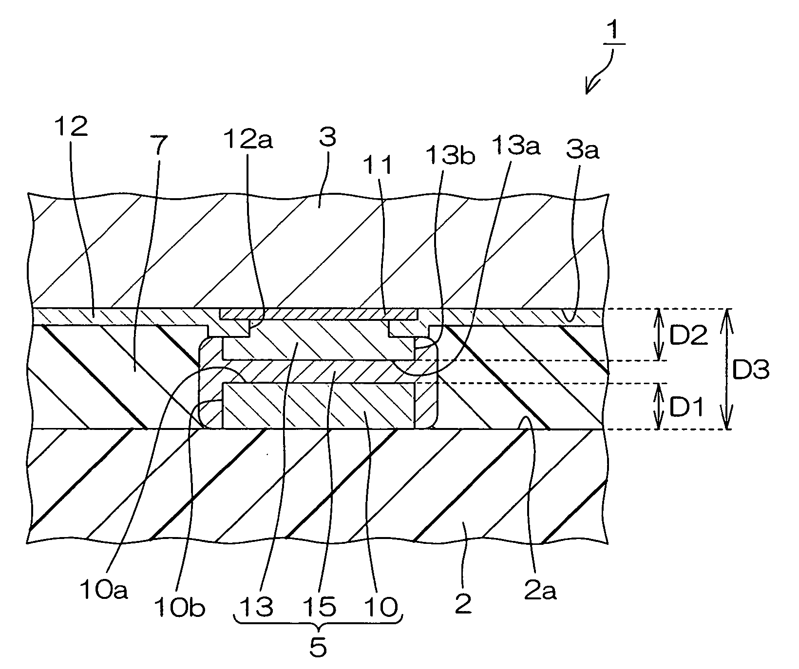
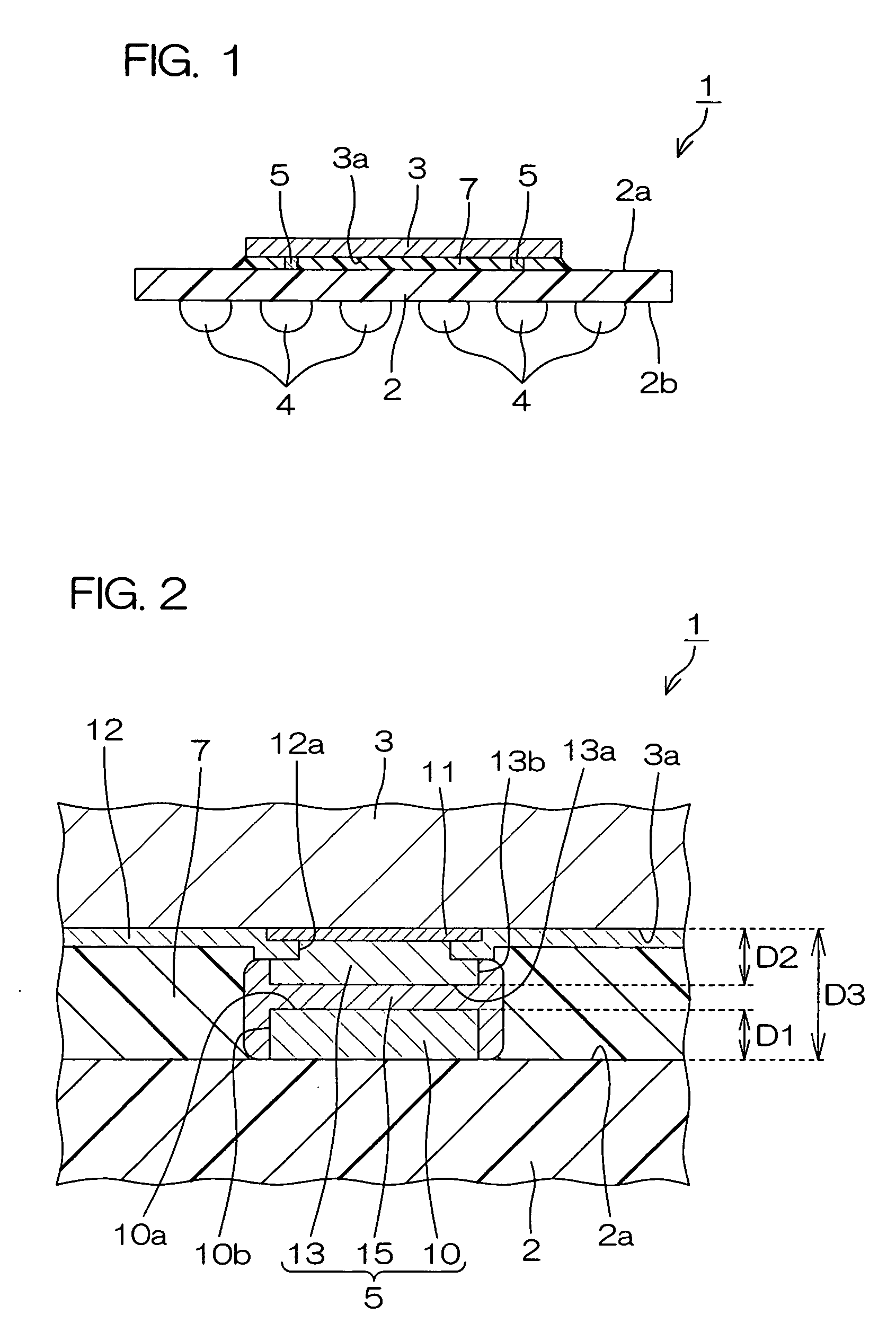
[0041]FIG. 1 is an illustrative sectional view showing a structure of a semiconductor device according to the invention.

[0042] The semiconductor device 1 includes: a wiring board 2 having a connection surface 2a; and a semiconductor chip 3 having a functional surface 3a formed with a functional element and connected to the connection structure 2a as directing its functional surface 3a to the connection surface 2a. The wiring board 2 and the semiconductor chip 3 are mechanically interconnected by means of a conductive member 5 in a manner to maintain a predetermined distance therebetween. The wiring board 2 and the semiconductor chip 3 are also electrically interconnected via the conductive member 5.

[0043] An underfill layer 7 formed from a resin material is interposed in the gap between the wiring board 2 and the semiconductor chip 3. The underfill layer 7 serves not only to protect the functional surface 3a and the conductive member 5 but also to reduce in-plane shear stress along...

second embodiment

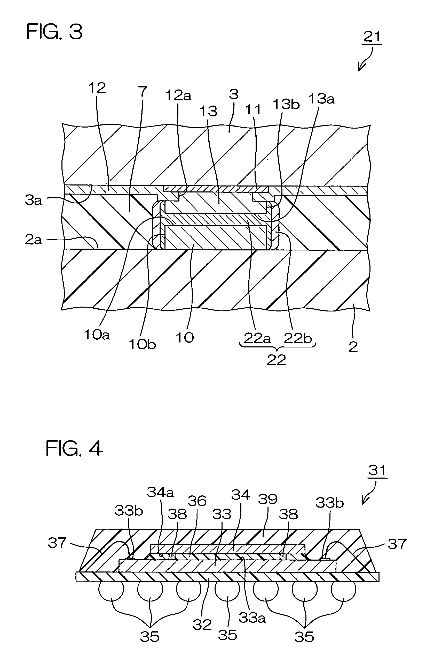
[0059]FIG. 3 is an illustrative sectional view showing a structure of a semiconductor device according to the invention. In FIG. 3, those parts corresponding to the individual parts shown in FIG. 2 are represented by the same reference characters as in FIG. 2, respectively.

[0060] This semiconductor device 21 includes a connecting member 22 in place of the connecting member 15 of the semiconductor device 1 shown in FIG. 2. The connecting member 22 includes: a reacted layer 22a filled in the gap between the connection pad 10 and the bump 13 and formed to cover the side face 10b of the connection pad 10 and the side face 13b of the bump 13; and an un-reacted layer 22b covering lateral sides of the reacted layer 22a.

[0061] The un-reacted layer 22b substantially consists of a low melting point metal (such as tin, lead, indium or an alloy thereof) having a lower solidus temperature than those of the other members of the semiconductor device 21, such as the connection pad 10 and bump 13. ...

third embodiment

[0065]FIG. 4 is an illustrative sectional view showing a structure of a semiconductor device according to the invention.

[0066] This semiconductor device 31 is a so-called multi-chip module and includes: a wiring board 32; a first semiconductor chip 33 overlaid thereon; and a second semiconductor chip 34 stacked on the first semiconductor chip 33. The first and second semiconductor chips 33, 34 respectively possess functional surfaces 33a, 34a each formed with a functional element. The first semiconductor chip 33 is mounted on the wiring board 32 in a so-called face-up state where the functional surface 33a is directed to the opposite side from the wiring board 32.

[0067] The second semiconductor chip 34 is connected to the first semiconductor chip 33 in a so-called face-down state where the functional surface 34a is directed to the functional surface 33a of the first semiconductor chip 33. That is, this semiconductor device 31 has a chip-on-chip structure. The first semiconductor ch...


PUM

PropertyMeasurementUnit
electrical resistivityaaaaaaaaaa
solidus temperatureaaaaaaaaaa
heightaaaaaaaaaa

Abstract

A semiconductor device is provided with: a solid device having a connection surface formed with a connection electrode projected therefrom; a semiconductor chip which has a functional surface formed with a metal bump projected therefrom and which is bonded to the connection surface of the solid device as directing its functional surface to the connection surface and maintaining a predetermined distance between the functional surface and the connection surface; and a connecting member containing a low melting point metal having a lower solidus temperature than that of the connection electrode and the bump, and interconnecting the connection electrode and the bump. A sum of a height of the connection electrode and a height of the bump is not less than a half of the predetermined distance.

Description

TECHNICAL FIELD [0001] The invention relates to a semiconductor device including a flip-chip bonded semiconductor chip. BACKGROUND ART [0002] A flip chip bonded structure for achieving size reduction and high-density mounting of semiconductor device has been receiving attention. The flip chip bonded structure has a structure wherein a semiconductor chip is connected to a solid device as directing its functional surface to the solid device, the functional surface being formed with a functional element. [0003]FIG. 7 is an illustrative sectional view showing a structure of a conventional semiconductor device having the flip chip bonded structure. The semiconductor device 51 includes: a wiring board 52 having a connection surface 52a; and a semiconductor chip 53 having a functional surface 53a formed with a functional element and connected to the connection surface 52a as directing its functional surface 53a to the connection surface 52a. [0004] The connection surface 52a of the wiring ...

Claims


Application Information

Patent Timeline
Patent Type & Authority Applications(United States)
IPC IPC(8): H01L23/488
CPCH01L23/49811H01L24/16H01L2224/13155H01L2224/13147H01L2224/13144H01L2224/13116H01L2224/13111H01L2224/13109H01L2924/014H01L2924/0105H01L2924/01006H01L2924/15311H01L2924/01327H01L2924/01322H01L2924/01082H01L24/81H01L25/0657H01L2224/13099H01L2224/13609H01L2224/16145H01L2224/16225H01L2224/48091H01L2224/48227H01L2224/73204H01L2224/8121H01L2224/81815H01L2224/83102H01L2224/92125H01L2225/06513H01L2924/01004H01L2924/01013H01L2924/01015H01L2924/01029H01L2924/01033H01L2924/01049H01L2924/01051H01L2924/01075H01L2924/01079H01L2924/00014H01L2924/181H01L2224/05027H01L2224/05022H01L2224/05573H01L2224/05568H01L2224/05001H01L2224/05624H01L2224/05644H01L2224/05647H01L24/05H01L24/13H01L2924/00H01L2224/05099H01L23/48
Inventor TANIDA, KAZUMASAMIYATA, OSAMU
Owner ROHM CO LTD
Why Eureka
Try Eureka