Method of Detecting Bio-Molecues Using the Same Field Effect Transistor on the Gate Sensing Surface
a field effect transistor and gate sensing technology, applied in the direction of porous material analysis, instruments, and semiconductor/solid-state device details, can solve the problems of insufficient sensing fets and reference fets, and achieve the effect of easy and accurate detection
- Summary
- Abstract
- Description
- Claims
- Application Information
AI Technical Summary
Benefits of technology
Problems solved by technology
Method used
Image
Examples
example 1
Preparation of a Field Effect Transistor Based Bio-Sensor
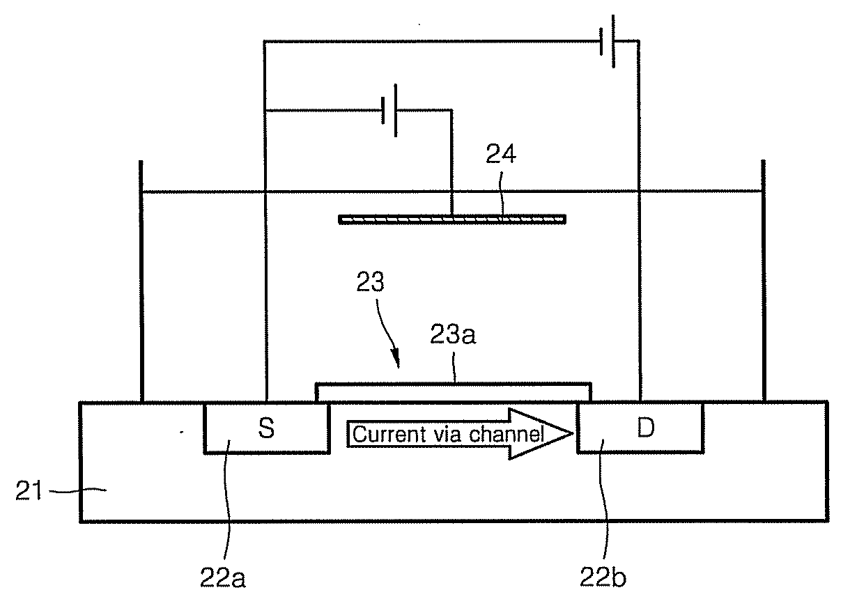
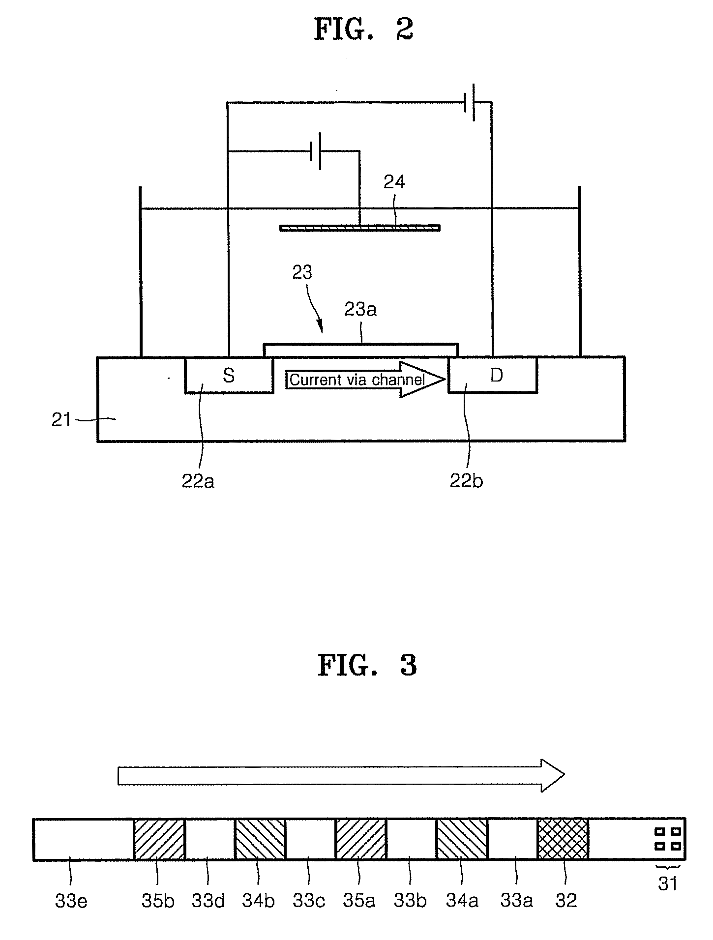
[0068]A field effect transistor device was prepared using a XC10-1.0 um CMOS process and equipment of X-FAB Semiconductor Foundries (Germany). A silicon oxide insulating layer 23 was formed on a channel between a source and a drain. The insulating layer 23 having a sensing surface 23a was formed by patterning the silicon oxide, and a reference electrode 24 disposed above and to be separate from the sensing surface 23a was formed to prepare a field effect transistor as illustrated in FIG. 2.
[0069]Then, the surface of the field effect transistor including the exposed sensing surface 23a and the reference electrode 24 was carefully washed with pure acetone and deionized water and dried. A wet station that is used in a semiconductor manufacturing process was used in washing the substrate. Then, the substrate was dried using a spin dry method.
example 2
Detection of PCR Products Using Field Effect Transistor Based Bio-Sensor
[0070]This example was conducted to determine whether a 4×12 field effect transistor based bio-sensor array manufactured in Example 1 could detect a PCR product.
[0071]For this, PCR products, a washing buffer, and a negative control (NTC) were alternatively brought into contact with the field effect transistor based bio-sensor.
[0072]FIG. 3 schematically illustrates a procedure of alternatively providing PCR products and a washing buffer, and a NTC between the sensing surface and the reference electrode of the field effect transistor of an embodiment of the present invention. Referring to FIG. 3, a calibrant solution 32, a washing solution 33a, a PCR product 34a, a washing solution 33b, an NTC 35a, a washing buffer 33c, a PCR product 34b, a washing solution 33d, an NTC 35b, and a washing buffer 33e are brought into contact with at least one field effect transistor based bio-sensor 31.
[0073]0.1 mM NaOAc was used as...
example 3
Detection of Concentration of PCR Products Using Field Effect Transistor Based Bio-Sensor
[0083]It was determined whether a field effect transistor based bio-sensor manufactured in Example 1 could detect the concentration of a PCR product.
[0084]For this, a plurality of PCR products, each having a different concentration, and a washing buffer were alternatively provided to the field effect transistor based bio-sensor.
[0085]FIG. 4A schematically illustrates a procedure of alternatively providing a plurality of PCR products, each having a different concentration and a washing buffer to the sensing surface of the field effect transistor of an embodiment of the present invention. Referring to FIG. 4A, 10 ng / μl of a PCR product 42, a washing solution 43a, 5 ng / μl of a PCR product 44, a washing solution 43b, 1 ng / μl of a PCR product 45, a washing solution 43c, 5 ng / μl of a PCR product 46, a washing solution 43d, 0.25 ng / μl of a PCR product 47, and a washing solution 43e were provided to at ...
PUM
| Property | Measurement | Unit |
|---|---|---|
| concentration | aaaaa | aaaaa |
| electric | aaaaa | aaaaa |
| polarity | aaaaa | aaaaa |
Abstract
Description
Claims
Application Information


