Method and structure for fabricating solar cells using a layer transfer process

a layer transfer and solar cell technology, applied in the field of method and structure for fabricating solar cells using a layer transfer process, can solve the problems of not possessing the optimum properties of highly effective solar cells, many limitations of solar cells, and difficult manufacturing of materials, so as to achieve a wider range of applicability

Inactive Publication Date: 2007-10-11
SILICON GENERAL CORPORATION
View PDF99 Cites 131 Cited by
  • Summary
  • Abstract
  • Description
  • Claims
  • Application Information

AI Technical Summary

Benefits of technology

[0006] According to embodiments of the present invention, techniques directed to the manufacture of photovoltaic materials are provided. More particularly, one embodiment of the invention provides a technique including a method and a structure for forming a solar cell structure using layer transfer techniques for photovoltaic applications. Certain embodiments in accordance with the present invention provide a thickening process using a silane type species having a desired deposition rate and thermal budget for the manufacture of photovoltaic devices. But it will be recognized that the invention has a wider range of applicability; and can also be applied to other types of applications such as for three-dimensional packaging of integrated semiconductor devices, photonic devices, piezoelectronic devices, flat panel displays, microelectromechanical systems (“MEMS”), nano-technology structures, sensors, actuators, integrated circuits, biological and biomedical devices, and the like.

Problems solved by technology

Unfortunately, such petroleum sources have become depleted and have lead to other problems.
Although effective, these solar cells still have many limitations.
These materials are often difficult to manufacture.
Although these plates may be formed effectively, they do not possess optimum properties for highly effective solar cells.
Such single crystal silicon is, however, expensive and is also difficult to use for solar applications in an efficient and cost effective manner.
Generally, thin-film solar cells are less expensive by using less silicon material but their amorphous or polycrystalline structure are less efficient than the more expensive bulk silicon cells made from single-crystal silicon substrates.

Method used


Image

  • Method and structure for fabricating solar cells using a layer transfer process
  • Method and structure for fabricating solar cells using a layer transfer process
  • Method and structure for fabricating solar cells using a layer transfer process

Examples


Embodiment Construction

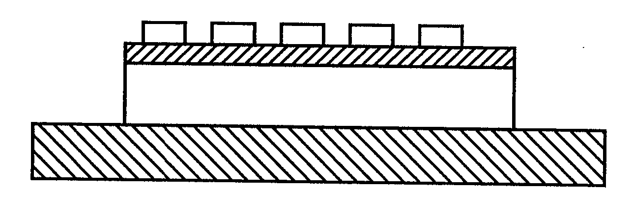
[0047] According to embodiments of the present invention, techniques directed to the manufacture of photovoltaic materials are provided. More particularly, one embodiment in accordance with the present invention provides a technique including a method and a structure for forming a solar cell structure using layer transfer techniques for photovoltaic applications. Other embodiments in accordance with the present invention provide a thickening process using a silane type species having a desired deposition rate and thermal budget for the manufacture of photovoltaic devices. While certain embodiments in accordance with the present invention may utilize di-silane or tri-silane type species, depending upon the particular embodiment other silane species can also be used. Depending upon the embodiment, deposition can occur using a variety of techniques including Atmospheric Pressure CVD (APCVD), Atomic Layer CVD (ALCVD) (e.g., Atomic Layer Epitaxy and Atomic layer deposition (ALD)), Aeroso...


PUM


Abstract

A photovoltaic cell device, e.g., solar cell, solar panel, and method of manufacture. The device has an optically transparent substrate comprises a first surface and a second surface. A first thickness of material (e.g., semiconductor material, single crystal material) having a first surface region and a second surface region is included. In a preferred embodiment, the surface region is overlying the first surface of the optically transparent substrate. The device has an optical coupling material provided between the first surface region of the thickness of material and the first surface of the optically transparent material. A second thickness of semiconductor material is overlying the second surface region to form a resulting thickness of semiconductor material.

Description

CROSS-REFERENCES TO RELATED APPLICATIONS [0001] The instant nonprovisional patent application claims priority to the following U.S. Provisional Patent Applications, all of which are incorporated by reference in their entirety herein for all purposes: Appl. No. 60 / 783,586 filed Mar. 17, 2006; Appl. No. 60 / 822,473 filed Aug. 15, 2006; Appl. No. 60 / 823,354 filed Aug. 23, 2006; and Appl. No. 60 / 823,356 filed Aug. 23, 2006.BACKGROUND OF THE INVENTION [0002] From the beginning of time, human beings have relied upon the “sun” to derive almost all useful forms of energy. Such energy comes from petroleum, radiant, wood, and various forms of thermal energy. As merely an example, human being have relied heavily upon petroleum sources such as coal and gas for much of their needs. Unfortunately, such petroleum sources have become depleted and have lead to other problems. As a replacement, in part, solar energy has been proposed to reduce our reliance on petroleum sources. As merely an example, s...

Claims


Application Information

Patent Timeline
Patent Type & Authority Applications(United States)
IPC IPC(8): H01L31/00
CPCH01L31/0232H01L31/0392H01L31/0725H01L31/0745Y02E10/547H01L31/1804H01L31/1872H01L31/1892H01L31/077H01L31/03925Y02P70/50
Inventor HENLEY, FRANCOIS J.ONG, PHILIP JAMES
Owner SILICON GENERAL CORPORATION
Why Eureka
Try Eureka